SLUS336A June 1998 – December 2016 UC1854 , UC2854 , UC3854
PRODUCTION DATA.
- 1 Features
- 2 Applications
- 3 Description
- 4 Revision History
- 5 Device Comparison Table
- 6 Pin Configuration and Functions
- 7 Specifications
- 8 Detailed Description
- 9 Application and Implementation
- 10Power Supply Recommendations
- 11Layout
- 12Device and Documentation Support
- 13Mechanical, Packaging, and Orderable Information
封装选项
请参考 PDF 数据表获取器件具体的封装图。
机械数据 (封装 | 引脚)
- DW|16
- N|16
散热焊盘机械数据 (封装 | 引脚)
- DW|16
订购信息
8 Detailed Description
8.1 Overview
The UC3854 provides active power factor correction for systems that otherwise would draw non-sinusoidal current from sinusoidal power lines. This device implements all the control functions necessary to build a power supply capable of optimally using available power-line current while minimizing line current distortion.
The UC3854 uses average current-mode control to accomplish fixed-frequency current control with stability and low distortion. The UC3854, with average current mode control, allows the boost stage to move between continuous and discontinuous modes of operation without a performance change. Unlike peak current-mode, average current control accurately maintains sinusoidal line current without slope compensation and with minimal response to noise transients.
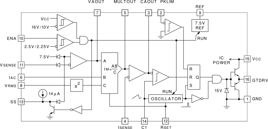
The UC3854 implements all the control functions necessary to build a power supply capable of optimally using available power-line current while minimizing line-current distortion. The UC3854 contains a voltage amplifier, an analog multiplier and divider, a current amplifier, and a fixed-frequency PWM. In addition, the UC3854 contains a power MOSFET compatible gate driver, 7.5-V reference, line anticipator, load-enable comparator, low-supply detector, and over-current comparator.
8.2 Functional Block Diagram

8.3 Feature Description
The UC3854 integrated circuit contains all the circuits necessary to control a power factor corrector. The UC3854 is designed to implement average current mode control but is flexible enough to be used for a wide variety of power topologies and control methods.
The top left corner, of the UC3854 block diagram, contains the under voltage lock out comparator and the enable comparator. The output of both of these comparators must be true to allow the device to operate. The inverting input to the voltage error amplifier is connected to pin VSENSE. The diodes shown around the voltage error amplifier are intended to represent the functioning of the internal circuits rather than to show the actual devices. The diodes shown in the block diagram are ideal diodes and indicate that the non-inverting input to the error amplifier is connected to the 7.5-V DC reference voltage under normal operation but is also used for the soft-start function. This configuration lets the voltage control loop begin operation before the output voltage has reached its operating point and eliminates the turn-on overshoot which plagues many power supplies. The diode shown between VSENSE and the inverting input of the error amplifier is also an ideal diode and is shown to eliminate confusion about whether there might be an extra diode drop added to the reference or not. In the actual device we do it with differential amplifiers. An internal current source is also provided for charging the soft-start timing capacitor.
The output of the voltage error amplifier is available on pin VAOUT, of the UC3854, and it is also an input to the multiplier. The other input to the multiplier is lAC, and this is the input for the programming wave shape from the input rectifiers. This pin is held, internally, at 6 V and is a current input. The feedforward input is VFF, and its value is squared before being fed into the divider input of the multiplier. The current (ISET) from the RSET pin is also used in the multiplier to limit the maximum output current. The output current of the multiplier is IMO and it flows out of pin MULTOUT which is also connected to the non-inverting input of the current error amplifier.
The inverting input of the current amplifier is connected to pin ISENSE. The output of the current error amplifier connects to the pulse width modulation (PWM) comparator where it is compared to the oscillator ramp on pin CT. The oscillator and the comparator drive the set-reset flip-flop which, in turn, drives the high current output on pin GTDRV. The output voltage is clamped internally to the UC3854 at 15 V so that power MOSFETs do not have their gates over driven. An emergency peak current limit is provided on pin PKLMT and it shuts off the output pulse when it is pulled slightly below ground. The reference voltage output is connected to pin VREF and the input voltage is connected to pin VCC.
8.4 Device Functional Modes
This device has no functional modes.