SLVS056P May 1976 – January 2015
PRODUCTION DATA.
- 1 Features
- 2 Applications
- 3 Description
- 4 Simplified Schematic
- 5 Revision History
- 6 Pin Configuration and Functions
-
7 Specifications
- 7.1 Absolute Maximum Ratings
- 7.2 ESD Ratings
- 7.3 Recommended Operating Conditions
- 7.4 Thermal Information
- 7.5 Electrical Characteristics — uA7805
- 7.6 Electrical Characteristics — uA7808
- 7.7 Electrical Characteristics — uA7810
- 7.8 Electrical Characteristics — uA7812
- 7.9 Electrical Characteristics — uA7815
- 7.10 Electrical Characteristics — uA7824
- 7.11 Typical Characteristics
- 8 Detailed Description
- 9 Application and Implementation
- 10Power Supply Recommendations
- 11Layout
- 12Device and Documentation Support
- 13Mechanical, Packaging, and Orderable Information
封装选项
机械数据 (封装 | 引脚)
散热焊盘机械数据 (封装 | 引脚)
- KTT|3
订购信息
7 Specifications
7.1 Absolute Maximum Ratings
over virtual junction temperature range (unless otherwise noted)| MIN | MAX | UNIT | |||
|---|---|---|---|---|---|
| Vl | Input voltage | μA7824C | 40 | V | |
| All others | 35 | ||||
| TJ | Operating virtual junction temperature | 150 | °C | ||
| Lead temperature | 1,6 mm (1/16 in) from case for 10 s | 260 | °C | ||
| Tstg | Storage temperature range | –65 | 150 | °C | |
7.2 ESD Ratings
| VALUE | UNIT | |||
|---|---|---|---|---|
| V(ESD) | Electrostatic discharge | Human body model (HBM), per ANSI/ESDA/JEDEC JS-001, all pins(1) | 3000 | V |
| Charged device model (CDM), per JEDEC specification JESD22-C101, all pins(2) | 2000 | |||
(1) JEDEC document JEP155 states that 500-V HBM allows safe manufacturing with a standard ESD control process.
(2) JEDEC document JEP157 states that 250-V CDM allows safe manufacturing with a standard ESD control process.
7.3 Recommended Operating Conditions
| MIN | MAX | UNIT | |||
|---|---|---|---|---|---|
| Vl | Input voltage | μA7805 | 7 | 25 | V |
| μA7808 | 10.5 | 25 | |||
| μA7810 | 12.5 | 28 | |||
| μA7812 | 14.5 | 30 | |||
| μA7815 | 17.5 | 30 | |||
| μA7824 | 27 | 38 | |||
| IO | Output current | 1.5 | A | ||
| TJ | Operating virtual junction temperature | 0 | 125 | °C | |
7.4 Thermal Information
| THERMAL METRIC(1) | μA78XX | UNIT | |||
|---|---|---|---|---|---|
| KTE | KCS, KCT, KC | KTT | |||
| 3 PINS | 3 PINS | 3 PINS | |||
| RθJA | Junction-to-ambient thermal resistance | 23 | 19 | 25.3 | °C/W |
| RθJC(top) | Junction-to-case (top) thermal resistance | 3 | 17 | 18 | |
| RθJP(top) | Junction-to-exposed-pad thermal resistance | 2.7 | 3 | 1.94 | |
(1) For more information about traditional and new thermal metrics, see the IC Package Thermal Metrics application report (SPRA953).
7.5 Electrical Characteristics — uA7805
at specified virtual junction temperature, VI = 10 V, IO = 500 mA (unless otherwise noted)| PARAMETER | TEST CONDITIONS | TJ(1) | μA7805C | UNIT | ||
|---|---|---|---|---|---|---|
| MIN | TYP | MAX | ||||
| Output voltage | IO = 5 mA to 1 A, VI = 7 V to 20 V, PD ≤ 15 W | 25°C | 4.8 | 5 | 5.2 | V |
| 0°C to 125°C | 4.75 | 5.25 | ||||
| Input voltage regulation | VI = 7 V to 25 V | 25°C | 3 | 100 | mV | |
| VI = 8 V to 12 V | 1 | 50 | ||||
| Ripple rejection(2) | VI = 8 V to 12 V, f = 120 Hz | 0°C to 125°C | 62 | 78 | dB | |
| VI = 8 V to 12 V, f = 120 Hz (KCT) | 68 | |||||
| Output voltage regulation | IO = 5 mA to 1.5 A | 25°C | 15 | 100 | mV | |
| IO = 250 mA to 750 mA | 5 | 50 | ||||
| Output resistance | f = 1 kHz | 0°C to 125°C | 0.017 | Ω | ||
| Temperature coefficient of output voltage | IO = 5 mA | 0°C to 125°C | –1.1 | mV/°C | ||
| Output noise voltage | f = 10 Hz to 100 kHz | 25°C | 40 | μV | ||
| Dropout voltage | IO = 1 A | 25°C | 2 | V | ||
| Bias current | 25°C | 4.2 | 8 | mA | ||
| Bias current change | VI = 7 V to 25 V | 0°C to 125°C | 1.3 | mA | ||
| IO = 5 mA to 1 A | 0.5 | |||||
| Short-circuit output current | 25°C | 750 | mA | |||
| Peak output current | 25°C | 2.2 | A | |||
(1) Pulse-testing techniques maintain the junction temperature as close to the ambient temperature as possible. Thermal effects must be taken into account separately. All characteristics are measured with a 0.33-μF capacitor across the input and a 0.1-μF capacitor across the output.
(2) This parameter is validated by design and verified during product characterization. It is not tested in production.
7.6 Electrical Characteristics — uA7808
at specified virtual junction temperature, VI = 14 V, IO = 500 mA (unless otherwise noted)| PARAMETER | TEST CONDITIONS | TJ(1) | μA7808C | UNIT | ||
|---|---|---|---|---|---|---|
| MIN | TYP | MAX | ||||
| Output voltage | IO = 5 mA to 1 A, VI = 10.5 V to 23 V, PD ≤ 15 W | 25°C | 7.7 | 8 | 8.3 | V |
| 0°C to 125°C | 7.6 | 8.4 | ||||
| Input voltage regulation | VI = 10.5 V to 25 V | 25°C | 6 | 160 | mV | |
| VI = 11 V to 17 V | 2 | 80 | ||||
| Ripple rejection(2) | VI = 11.5 V to 21.5 V, f = 120 Hz | 0°C to 125°C | 55 | 72 | dB | |
| VI = 11.5 V to 21.5 V, f = 120 Hz (KCT) | 62 | |||||
| Output voltage regulation | IO = 5 mA to 1.5 A | 25°C | 12 | 160 | mV | |
| IO = 250 mA to 750 mA | 4 | 80 | ||||
| Output resistance | f = 1 kHz | 0°C to 125°C | 0.016 | Ω | ||
| Temperature coefficient of output voltage | IO = 5 mA | 0°C to 125°C | –0.8 | mV/°C | ||
| Output noise voltage | f = 10 Hz to 100 kHz | 25°C | 52 | μV | ||
| Dropout voltage | IO = 1 A | 25°C | 2 | V | ||
| Bias current | 25°C | 4.3 | 8 | mA | ||
| Bias current change | VI = 10.5 V to 25 V | 0°C to 125°C | 1 | mA | ||
| IO = 5 mA to 1 A | 0.5 | |||||
| Short-circuit output current | 25°C | 450 | mA | |||
| Peak output current | 25°C | 2.2 | A | |||
(1) Pulse-testing techniques maintain the junction temperature as close to the ambient temperature as possible. Thermal effects must be taken into account separately. All characteristics are measured with a 0.33-μF capacitor across the input and a 0.1-μF capacitor across the output.
(2) This parameter is validated by design and verified during product characterization. It is not tested in production.
7.7 Electrical Characteristics — uA7810
at specified virtual junction temperature, VI = 17 V, IO = 500 mA (unless otherwise noted)| PARAMETER | TEST CONDITIONS | TJ(1) | μA7810C | UNIT | ||
|---|---|---|---|---|---|---|
| MIN | TYP | MAX | ||||
| Output voltage | IO = 5 mA to 1 A, VI = 12.5 V to 25 V, PD ≤ 15 W | 25°C | 9.6 | 10 | 10.4 | V |
| 0°C to 125°C | 9.5 | 10.5 | ||||
| Input voltage regulation | VI = 12.5 V to 28 V | 25°C | 7 | 200 | mV | |
| VI = 14 V to 20 V | 2 | 100 | ||||
| Ripple rejection(2) | VI = 13 V to 23 V, f = 120 Hz | 0°C to 125°C | 55 | 71 | dB | |
| Output voltage regulation | IO = 5 mA to 1.5 A | 25°C | 12 | 200 | mV | |
| IO = 250 mA to 750 mA | 4 | 100 | ||||
| Output resistance | f = 1 kHz | 0°C to 125°C | 0.018 | Ω | ||
| Temperature coefficient of output voltage | IO = 5 mA | 0°C to 125°C | –1 | mV/°C | ||
| Output noise voltage | f = 10 Hz to 100 kHz | 25°C | 70 | μV | ||
| Dropout voltage | IO = 1 A | 25°C | 2 | V | ||
| Bias current | 25°C | 4.3 | 8 | mA | ||
| Bias current change | VI = 12.5 V to 28 V | 0°C to 125°C | 1 | mA | ||
| IO = 5 mA to 1 A | 0.5 | |||||
| Short-circuit output current | 25°C | 400 | mA | |||
| Peak output current | 25°C | 2.2 | A | |||
(1) Pulse-testing techniques maintain the junction temperature as close to the ambient temperature as possible. Thermal effects must be taken into account separately. All characteristics are measured with a 0.33-μF capacitor across the input and a 0.1-μF capacitor across the output.
(2) This parameter is validated by design and verified during product characterization. It is not tested in production.
7.8 Electrical Characteristics — uA7812
at specified virtual junction temperature, VI = 19 V, IO = 500 mA (unless otherwise noted)| PARAMETER | TEST CONDITIONS | TJ(1) | μA7812C | UNIT | ||
|---|---|---|---|---|---|---|
| MIN | TYP | MAX | ||||
| Output voltage | IO = 5 mA to 1 A, VI = 14.5 V to 27 V, PD ≤ 15 W | 25°C | 11.5 | 12 | 12.5 | V |
| 0°C to 125°C | 11.4 | 12.6 | ||||
| Input voltage regulation | VI = 14.5 V to 30 V | 25°C | 10 | 240 | mV | |
| VI = 16 V to 22 V | 3 | 120 | ||||
| Ripple rejection(2) | VI = 15 V to 25 V, f = 120 Hz | 0°C to 125°C | 55 | 71 | dB | |
| VI = 15 V to 25 V, f = 120 Hz (KCT) | 61 | |||||
| Output voltage regulation | IO = 5 mA to 1.5 A | 25°C | 12 | 240 | mV | |
| IO = 250 mA to 750 mA | 4 | 120 | ||||
| Output resistance | f = 1 kHz | 0°C to 125°C | 0.018 | Ω | ||
| Temperature coefficient of output voltage | IO = 5 mA | 0°C to 125°C | –1 | mV/°C | ||
| Output noise voltage | f = 10 Hz to 100 kHz | 25°C | 75 | μV | ||
| Dropout voltage | IO = 1 A | 25°C | 2 | V | ||
| Bias current | 25°C | 4.3 | 8 | mA | ||
| Bias current change | VI = 14.5 V to 30 V | 0°C to 125°C | 1 | mA | ||
| IO = 5 mA to 1 A | 0.5 | |||||
| Short-circuit output current | 25°C | 350 | mA | |||
| Peak output current | 25°C | 2.2 | A | |||
(1) Pulse-testing techniques maintain the junction temperature as close to the ambient temperature as possible. Thermal effects must be taken into account separately. All characteristics are measured with a 0.33-μF capacitor across the input and a 0.1-μF capacitor across the output.
(2) This parameter is validated by design and verified during product characterization. It is not tested in production.
7.9 Electrical Characteristics — uA7815
at specified virtual junction temperature, VI = 23 V, IO = 500 mA (unless otherwise noted)| PARAMETER | TEST CONDITIONS | TJ(1) | μA7815C | UNIT | ||
|---|---|---|---|---|---|---|
| MIN | TYP | MAX | ||||
| Output voltage | IO = 5 mA to 1 A, VI = 17.5 V to 30 V, PD ≤ 15 W | 25°C | 14.4 | 15 | 15.6 | V |
| 0°C to 125°C | 14.25 | 15.75 | ||||
| Input voltage regulation | VI = 17.5 V to 30 V | 25°C | 11 | 300 | mV | |
| VI = 20 V to 26 V | 3 | 150 | ||||
| Ripple rejection(2) | VI = 18.5 V to 28.5 V, f = 120 Hz | 0°C to 125°C | 54 | 70 | dB | |
| VI = 18.5 V to 28.5 V, f = 120 Hz (KCT) | 60 | |||||
| Output voltage regulation | IO = 5 mA to 1.5 A | 25°C | 12 | 300 | mV | |
| IO = 250 mA to 750 mA | 4 | 150 | ||||
| Output resistance | f = 1 kHz | 0°C to 125°C | 0.019 | Ω | ||
| Temperature coefficient of output voltage | IO = 5 mA | 0°C to 125°C | –1 | mV/°C | ||
| Output noise voltage | f = 10 Hz to 100 kHz | 25°C | 90 | μV | ||
| Dropout voltage | IO = 1 A | 25°C | 2 | V | ||
| Bias current | 25°C | 4.4 | 8 | mA | ||
| Bias current change | VI = 17.5 V to 30 V | 0°C to 125°C | 1 | mA | ||
| IO = 5 mA to 1 A | 0.5 | |||||
| Short-circuit output current | 25°C | 230 | mA | |||
| Peak output current | 25°C | 2.1 | A | |||
(1) Pulse-testing techniques maintain the junction temperature as close to the ambient temperature as possible. Thermal effects must be taken into account separately. All characteristics are measured with a 0.33-μF capacitor across the input and a 0.1-μF capacitor across the output.
(2) This parameter is validated by design and verified during product characterization. It is not tested in production.
7.10 Electrical Characteristics — uA7824
at specified virtual junction temperature, VI = 33 V, IO = 500 mA (unless otherwise noted)| PARAMETER | TEST CONDITIONS | TJ(1) | μA7824C | UNIT | ||
|---|---|---|---|---|---|---|
| MIN | TYP | MAX | ||||
| Output voltage | IO = 5 mA to 1 A, VI = 27 V to 38 V, PD ≤ 15 W | 25°C | 23 | 24 | 25 | V |
| 0°C to 125°C | 22.8 | 25.2 | ||||
| Input voltage regulation | VI = 27 V to 38 V | 25°C | 18 | 480 | mV | |
| VI = 30 V to 36 V | 6 | 240 | ||||
| Ripple rejection(2) | VI = 28 V to 38 V, f = 120 Hz | 0°C to 125°C | 50 | 66 | dB | |
| Output voltage regulation | IO = 5 mA to 1.5 A | 25°C | 12 | 480 | mV | |
| IO = 250 mA to 750 mA | 4 | 240 | ||||
| Output resistance | f = 1 kHz | 0°C to 125°C | 0.028 | Ω | ||
| Temperature coefficient of output voltage | IO = 5 mA | 0°C to 125°C | –1.5 | mV/°C | ||
| Output noise voltage | f = 10 Hz to 100 kHz | 25°C | 170 | μV | ||
| Dropout voltage | IO = 1 A | 25°C | 2 | V | ||
| Bias current | 25°C | 4.6 | 8 | mA | ||
| Bias current change | VI = 27 V to 38 V | 0°C to 125°C | 1 | mA | ||
| IO = 5 mA to 1 A | 0.5 | |||||
| Short-circuit output current | 25°C | 150 | mA | |||
| Peak output current | 25°C | 2.1 | A | |||
(1) Pulse-testing techniques maintain the junction temperature as close to the ambient temperature as possible. Thermal effects must be taken into account separately. All characteristics are measured with a 0.33-μF capacitor across the input and a 0.1-μF capacitor across the output.
(2) This parameter is validated by design and verified during product characterization. It is not tested in production.
7.11 Typical Characteristics
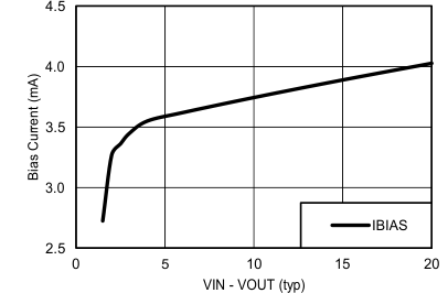 Figure 1. µA7805 Bias Current vs Voltage Differential at 25°C