ZHCSI29B June   2017  – May 2019 TUSB1046A-DCI

PRODUCTION DATA.  

  1. 特性
  2. 应用
  3. 说明
    1.     Device Images
      1.      简化电路原理图
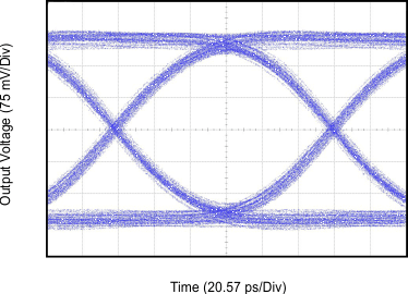
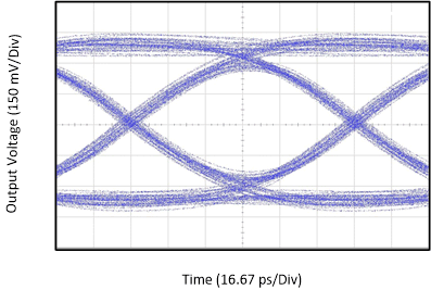
      2.      TUSB1046A-DCI 眼图
  4. 修订历史记录
  5. Pin Configuration and Functions
    1.     Pin Functions
  6. Specifications
    1. 6.1  Absolute Maximum Ratings
    2. 6.2  ESD Ratings
    3. 6.3  Recommended Operating Conditions
    4. 6.4  Thermal Information
    5. 6.5  Power Supply Characteristics
    6. 6.6  DC Electrical Characteristics
    7. 6.7  AC Electrical Characteristics
    8. 6.8  DCI Specific Electrical Characteristics
    9. 6.9  Timing Requirements
    10. 6.10 Switching Characteristics
    11. 6.11 Typical Characteristics
  7. Parameter Measurement Information
  8. Detailed Description
    1. 8.1 Overview
    2. 8.2 Functional Block Diagram
    3. 8.3 Feature Description
      1. 8.3.1 USB 3.1
      2. 8.3.2 DisplayPort
      3. 8.3.3 4-level Inputs
      4. 8.3.4 Receiver Linear Equalization
    4. 8.4 Device Functional Modes
      1. 8.4.1 Device Configuration in GPIO Mode
      2. 8.4.2 Device Configuration In I2C Mode
      3. 8.4.3 DisplayPort Mode
      4. 8.4.4 Linear EQ Configuration
      5. 8.4.5 USB3.1 Modes
      6. 8.4.6 Operation Timing – Power Up
    5. 8.5 Programming
    6. 8.6 Register Maps
      1. 8.6.1 General Register (address = 0x0A) [reset = 00000001]
        1. Table 11. General Registers
      2. 8.6.2 DisplayPort Control/Status Registers (address = 0x10) [reset = 00000000]
        1. Table 12. DisplayPort Control/Status Registers (0x10)
      3. 8.6.3 DisplayPort Control/Status Registers (address = 0x11) [reset = 00000000]
        1. Table 13. DisplayPort Control/Status Registers (0x11)
      4. 8.6.4 DisplayPort Control/Status Registers (address = 0x12) [reset = 00000000]
        1. Table 14. DisplayPort Control/Status Registers (0x12)
      5. 8.6.5 DisplayPort Control/Status Registers (address = 0x13) [reset = 00000000]
        1. Table 15. DisplayPort Control/Status Registers (0x13)
      6. 8.6.6 USB3.1 Control/Status Registers (address = 0x20) [reset = 00000000]
        1. Table 16. USB3.1 Control/Status Registers (0x20)
      7. 8.6.7 USB3.1 Control/Status Registers (address = 0x21) [reset = 00000000]
        1. Table 17. USB3.1 Control/Status Registers (0x21)
      8. 8.6.8 USB3.1 Control/Status Registers (address = 0x22) [reset = 00000100]
        1. Table 18. USB3.1 Control/Status Registers (0x22)
  9. Application and Implementation
    1. 9.1 Application Information
    2. 9.2 Typical Application
      1. 9.2.1 Design Requirements
      2. 9.2.2 Detailed Design Procedure
      3. 9.2.3 Application Curve
    3. 9.3 System Examples
      1. 9.3.1 USB 3.1 Only
      2. 9.3.2 USB 3.1 and 2 Lanes of DisplayPort
      3. 9.3.3 DisplayPort Only
  10. 10Power Supply Recommendations
  11. 11Layout
    1. 11.1 Layout Guidelines
    2. 11.2 Layout Example
  12. 12器件和文档支持
    1. 12.1 相关链接
    2. 12.2 接收文档更新通知
    3. 12.3 社区资源
    4. 12.4 商标
    5. 12.5 静电放电警告
    6. 12.6 术语表
  13. 13机械、封装和可订购信息

封装选项

机械数据 (封装 | 引脚)
散热焊盘机械数据 (封装 | 引脚)
订购信息

Typical Characteristics

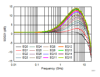
TUSB1046A-DCI D001_SLLSEV7.gif
Figure 1. DisplayPort EQ Settings Curves
TUSB1046A-DCI D003_SLLSEV7.gif
Figure 3. USB TX EQ Settings Curves
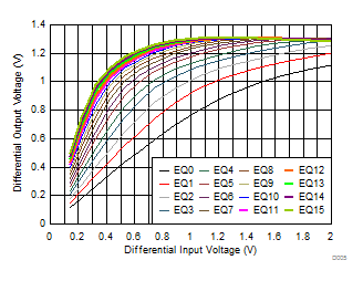
TUSB1046A-DCI D005_SLLSEW2.gif
Figure 5. USB TX Linearity Curves at 5 GHz
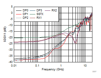
TUSB1046A-DCI D007_SLLSEV7.gif
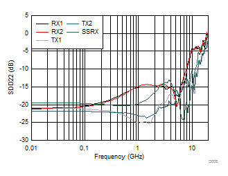
Figure 7. Input Return Loss Performance
TUSB1046A-DCI G001_SLLSEV7.gif
Figure 9. DisplayPort HBR3 Eye-Pattern Performance with 12-inch Input PCB Trace at 8.1 Gbps
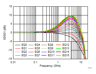
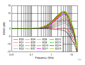
TUSB1046A-DCI D002_SLLSEV7.gif
Figure 2. USB RX EQ Settings Curves
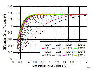
TUSB1046A-DCI D004_SLLSEV7.gif
Figure 4. DisplayPort Linearity Curves at 4.05 GHz
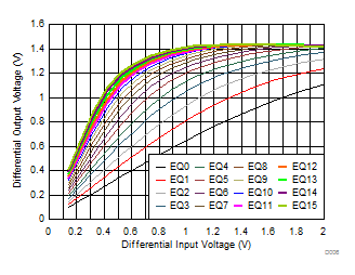
TUSB1046A-DCI D006_SLLSEW2.gif
Figure 6. USB RX Linearity Curves at 5 GHz
TUSB1046A-DCI D008_SLLSEV7.gif
Figure 8. Output Return Loss Performance
TUSB1046A-DCI TUSB1046A_DCI_10G_USB_Eye.gif
Figure 10. USB 3.1 Gen2 Eye-Pattern Performance with
12-inch Input PCB Trace at 10 Gbps