ZHCSF59A October   2014  – July 2016 TS5A22364-Q1

PRODUCTION DATA.  

  1. 特性
  2. 应用
  3. 说明
  4. 修订历史记录
  5. Pin Configuration and Functions
  6. Specifications
    1. 6.1 Absolute Maximum Ratings
    2. 6.2 ESD Ratings
    3. 6.3 Recommended Operating Conditions
    4. 6.4 Thermal Information
    5. 6.5 Electrical Characteristics—2.5-V Supply
    6. 6.6 Electrical Characteristics—3.3-V Supply
    7. 6.7 Electrical Characteristics—5-V Supply
    8. 6.8 Typical Characteristics
  7. Parameter Measurement Information
  8. Detailed Description
    1. 8.1 Overview
    2. 8.2 Functional Block Diagram
    3. 8.3 Feature Description
      1. 8.3.1 Click-and-Pop Reduction
    4. 8.4 Device Functional Modes
  9. Application and Implementation
    1. 9.1 Application Information
      1. 9.1.1 Negative Signal Swing Capability
    2. 9.2 Typical Application
      1. 9.2.1 Design Requirements
      2. 9.2.2 Detailed Design Procedure
      3. 9.2.3 Application Curve
  10. 10Power Supply Recommendations
  11. 11Layout
    1. 11.1 Layout Guidelines
    2. 11.2 Layout Example
  12. 12器件和文档支持
    1. 12.1 接收文档更新通知
    2. 12.2 社区资源
    3. 12.3 商标
    4. 12.4 静电放电警告
  13. 13机械、封装和可订购信息

封装选项

机械数据 (封装 | 引脚)
散热焊盘机械数据 (封装 | 引脚)
订购信息

5 Pin Configuration and Functions

DGS Package
10-Pin VSSOP
Top View
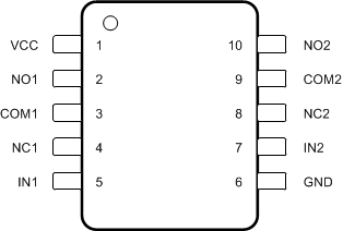
TS5A22364-Q1 PinOut_01_SCDS361.gif

Pin Functions

PIN I/O DESCRIPTION
NO. NAME
1 VCC I Supply power
2 NO1 I/O Normally open (NO) signal path, switch 1
3 COM1 I/O Common signal path, switch 1
4 NC1 I/O Normally closed (NC) signal path, switch 1
5 IN1 I Digital control pin to connect COM1 to NO1, switch 1
6 GND Ground
7 IN2 I Digital control pin to connect COM2 to NO2, switch 2
8 NC2 I/O Normally closed (NC) signal path, switch 2
9 COM2 I/O Common signal path, switch 2
10 NO2 I/O Normally open (NO) signal path, switch 2