ZHCSD70B November 2014 – February 2015 TS3A227E
PRODUCTION DATA.
- 1 特性
- 2 应用范围
- 3 说明
- 4 简化电路原理图
- 5 修订历史记录
- 6 Pin Configuration and Functions
- 7 Specifications
- 8 Parameter Measurement Information
-
9 Detailed Description
- 9.1 Overview
- 9.2 Functional Block Diagram
- 9.3 Feature Description
- 9.4 Device Functional Modes
- 9.5 Register Maps
- 9.6
Register Field Descriptions
- 9.6.1 Device ID Register Field Descriptions (Address 00h)
- 9.6.2 Interrupt Register Field Descriptions (Address 01h)
- 9.6.3 Key Press Interrupt Register Field Descriptions (Address 02h)
- 9.6.4 Interrupt Disable Register Field Descriptions (Address 03h)
- 9.6.5 Device Settings Field Descriptions (Address 04h)
- 9.6.6 Key Press Settings 1 Field Descriptions (Address 05h)
- 9.6.7 Key Press Settings 2 Field Descriptions (Address 06h)
- 9.6.8 Switch Control 1 Field Descriptions (Address 07h)
- 9.6.9 Switch Control 2 Field Descriptions (Address 08h)
- 9.6.10 Switch Status 1 Field Descriptions (Address 09h)
- 9.6.11 Switch Status 2 Field Descriptions (Address 0Ah)
- 9.6.12 Detection Results Field Descriptions (Address 0Bh)
- 9.6.13 ADC Output Field Descriptions (Address 0Ch)
- 9.6.14 Threshold 1 Field Descriptions (Address 0Dh)
- 9.6.15 Threshold 2 Field Descriptions (Address 0Eh)
- 9.6.16 Threshold 3 Field Descriptions (Address 0Fh)
- 10Application and Implementation
- 11Power Supply Recommendations
- 12Layout
- 13器件和文档支持
- 14机械封装和可订购信息
12 Layout
12.1 Layout Guidelines
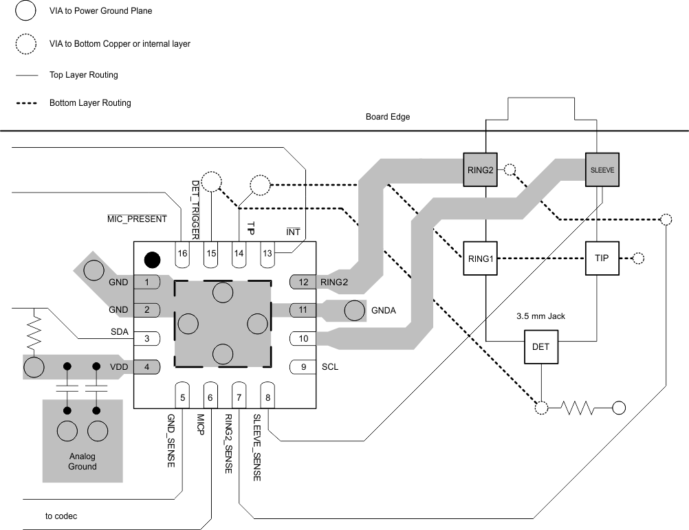
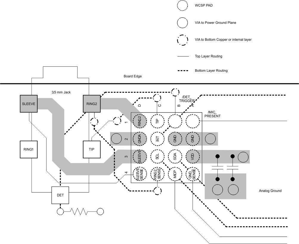
- The VDD pin must have de-coupling capacitors places as closely to the device as possible. Typically recommended capacitors are a 0.1 µF and 1 µF capacitor.
- If FM support is not needed connect GNDA to system GND along with the GND connections with the shortest connections possible.
- RING2 and SLEEVE should be routed on the same layer as the audio jack for best performance with less than 50 mΩ to the audio jack pins. These two pins should have priority in layout over other pins. It is recommended to not use vias on these traces and pair the device with an audio jack that facilitates this type of layout.
- The RING2_SENSE and SLEEVE_SENSE pins are kelvin connections to the audio jack and should be shorted to RING2 and SLEEVE as close to the audio jack as possible. If there are 0 Ω resistors between the SLEEVE/RING2 pins and the jack, connect the SENSE lines to the jack sleeve and ring2 contacts. If a microphone is connected one of the SENSE lines will carry the microphone signal and the MICBIAS supply. It is recommended that these traces not have more than 1 Ω impedance to the jack.
- Route the I2C and digital signals away from the audio signals to prevent coupling onto the audio lines.
12.2 Layout Example (QFN)
 Figure 35. QFN Layout Example
12.3 Layout Example (DSBGA)
 Figure 36. DSBGA Layout Example