SLWS230E September   2011  – December 2015 TRF3765

PRODUCTION DATA.  

  1. Features
  2. Applications
  3. Description
  4. Revision History
  5. Pin Configuration and Functions
  6. Specifications
    1. 6.1 Absolute Maximum Ratings
    2. 6.2 ESD Ratings
    3. 6.3 Recommended Operating Conditions
    4. 6.4 Thermal Information
    5. 6.5 Electrical Characteristics
    6. 6.6 4WI Timing: Write Operation
    7. 6.7 Readback 4WI Timing
    8. 6.8 Typical Characteristics
  7. Detailed Description
    1. 7.1 Overview
    2. 7.2 Functional Block Diagram
    3. 7.3 Feature Description
      1. 7.3.1 Lock Detect
      2. 7.3.2 LO Divider
      3. 7.3.3 Selecting the VCO and VCO Frequency Control
      4. 7.3.4 External VCO
    4. 7.4 Device Functional Modes
      1. 7.4.1 VCO_TEST_MODE
      2. 7.4.2 Readback Mode
      3. 7.4.3 Integer and Fractional Mode Selection
      4. 7.4.4 PLL Architecture
        1. 7.4.4.1 Selecting PLL Divider Values
        2. 7.4.4.2 Setup Example for Integer Mode
        3. 7.4.4.3 Setup Example for Fractional Mode
      5. 7.4.5 Fractional Mode Setup
    5. 7.5 Register Maps
      1. 7.5.1 PLL 4WI Registers
        1. 7.5.1.1 Register 1
          1. 7.5.1.1.1 CAL_CLK_SEL[3..0]
          2. 7.5.1.1.2 ICP[4..0]
        2. 7.5.1.2 Register 2
          1. 7.5.1.2.1 PLL_DIV <1.0>
          2. 7.5.1.2.2 VCOSEL_MODE
        3. 7.5.1.3 Register 3
        4. 7.5.1.4 Register 4
        5. 7.5.1.5 Register 5
        6. 7.5.1.6 Register 6
      2. 7.5.2 Readback from the Internal Register Banks
        1. 7.5.2.1 Register 0 Write
          1. 7.5.2.1.1 Register 0 Read
  8. Application and Implementation
    1. 8.1 Application Information
    2. 8.2 Typical Application
      1. 8.2.1 Design Requirements
      2. 8.2.2 Detailed Design Procedures
        1. 8.2.2.1 Power Supply
        2. 8.2.2.2 Loop Filter
        3. 8.2.2.3 Reference Clock
      3. 8.2.3 Application Curves
  9. Power Supply Recommendations
  10. 10Layout
    1. 10.1 Layout Guidelines
    2. 10.2 Layout Example
  11. 11Device and Documentation Support
    1. 11.1 Trademarks
    2. 11.2 Electrostatic Discharge Caution
    3. 11.3 Glossary
  12. 12Mechanical, Packaging, and Orderable Information

封装选项

机械数据 (封装 | 引脚)
散热焊盘机械数据 (封装 | 引脚)
订购信息

10 Layout

10.1 Layout Guidelines

Layout of the application board significantly impacts the analog performance of the TRF3765 device. Noise and high-speed signals should be prevented from leaking onto power-supply pins or analog signals. Follow these recommendations:

  • Place supply decoupling capacitors physically close to the device, on the same side of the board. Each supply pin should be isolated with a ferrite bead.
  • Maintain a continuous ground plane in the vicinity of the device and as return paths for all high-speed signal lines. Place reference plane vias or decoupling capacitors near any signal line reference transition.
  • The pad on the bottom of the device must be electrically grounded. Connect GND pins directly to the pad on the surface layer. Connect the GND pins and pad directly to surface ground where possible.
  • Power planes should not overlap each other or high-speed signal lines.
  • Isolate REF_IN routing from loop filter lines, control lines, and other high-speed lines.

See Figure 80 for an example of critical component layout (for the top PCB layer).

10.2 Layout Example
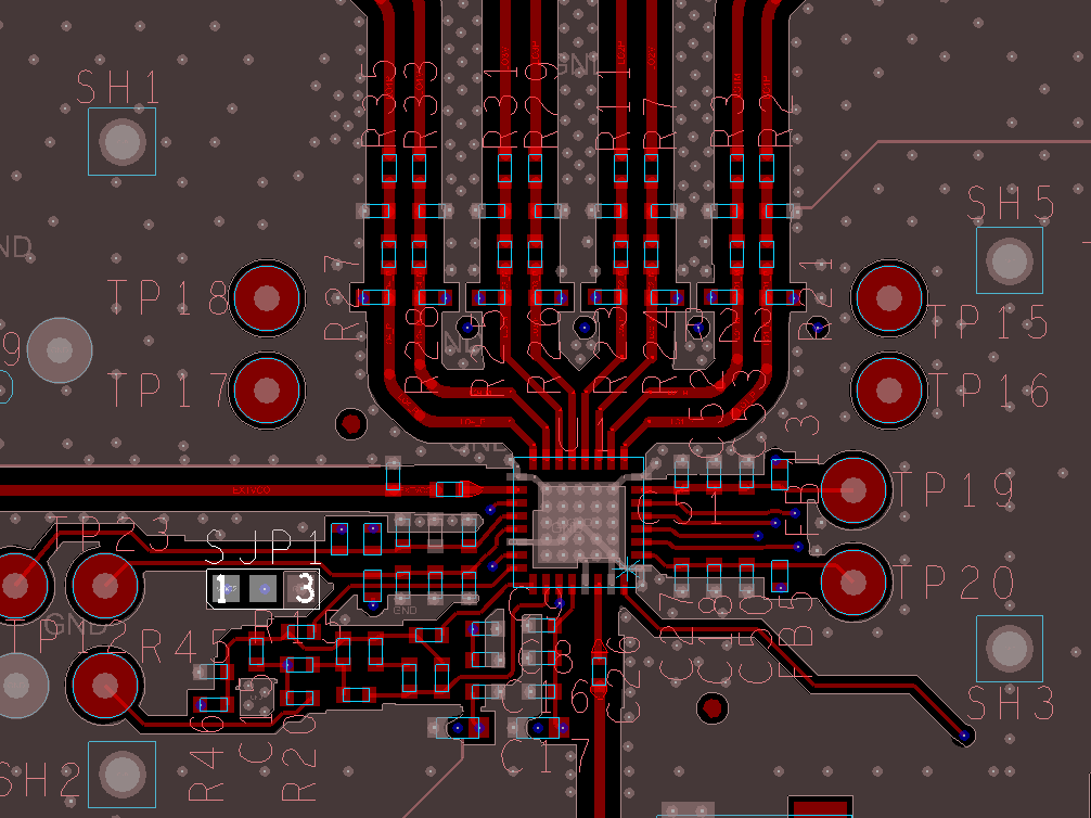
TRF3765 TRF3765_Layout.png Figure 80. Layout of Critical TRF3765 Components