ZHCSPZ6B February 2022 – November 2022 TPSM82903
PRODUCTION DATA
- 1 特性
- 2 应用
- 3 说明
- 4 Revision History
- 5 Pin Configuration and Functions
- 6 Specifications
-
7 Detailed Description
- 7.1 Overview
- 7.2 Functional Block Diagram
- 7.3
Feature Description
- 7.3.1 Mode Selection and Device Configuration (MODE/S-CONF)
- 7.3.2 Adjustable VO Operation (External Voltage Divider)
- 7.3.3 Setable VO Operation (VSET and Internal Voltage Divider)
- 7.3.4 Soft Start/Tracking (SS/TR)
- 7.3.5 Smart Enable with Precise Threshold
- 7.3.6 Power Good (PG)
- 7.3.7 Undervoltage Lockout (UVLO)
- 7.3.8 Current Limit And Short Circuit Protection
- 7.3.9 Thermal Shutdown
- 7.4 Device Functional Modes
- 8 Application and Implementation
- 9 Device and Documentation Support
- 10Mechanical, Packaging, and Orderable Information
8.2.2.2 Programming the Output Voltage
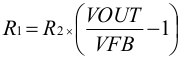
The output voltage of the TPSM82903 is adjustable. It can be programmed for output voltages from 0.6 V to 5.5 V using a resistor divider from VOUT to GND. The voltage at the FB pin is regulated to 600 mV. The value of the output voltage is set by the selection of the resistor divider from Equation 10. It is recommended to choose resistor values that allow a current of at least 2 μA, meaning the value of R2 must not exceed 400 kΩ. Lower resistor values are recommended for highest accuracy and most robust design.
With typical VFB = 0.6 V, 1-MHz switching frequency is not recommended for VOUT > 1.8 V.
| Nominal Output Voltage | R1 | R2 | Exact Output Voltage |
|---|---|---|---|
| 0.75 V | 24.9 kΩ | 100 kΩ | 0.749 V |
| 1.2 V | 100 kΩ | 100 kΩ | 1.2 V |
| 1.5 V | 150 kΩ | 100 kΩ | 1.5 V |
| 1.8 V | 200 kΩ | 100 kΩ | 1.8 V |
| 2.0 V | 49.9 kΩ | 21.5 kΩ | 1.992 V |
| 2.5 V | 100 kΩ | 31.6 kΩ | 2.498 V |
| 3.0 V | 100 kΩ | 24.9 kΩ | 3.009 V |
| 3.3 V | 113 kΩ | 24.9 kΩ | 3.322 V |
| 5.0 V | 182 kΩ | 24.9 kΩ | 4.985 V |