ZHCSK69F August   2019  – November 2021 TPSM82821 , TPSM82821A , TPSM82822 , TPSM82822A , TPSM82823 , TPSM82823A

PRODUCTION DATA  

  1. 特性
  2. 应用
  3. 说明
  4. Revision History
  5. Device Comparison Table
  6. Pin Configuration and Functions
  7. Specifications
    1. 7.1 Absolute Maximum Ratings
    2. 7.2 ESD Ratings
    3. 7.3 Recommended Operating Conditions
    4. 7.4 Thermal Information
    5. 7.5 Electrical Characteristics
    6. 7.6 Typical Characteristics
  8. Detailed Description
    1. 8.1 Overview
    2. 8.2 Functional Block Diagram
    3. 8.3 Feature Description
      1. 8.3.1 PWM and PSM Operation
      2. 8.3.2 Low Dropout Operation (100% Duty Cycle)
      3. 8.3.3 Soft Start-up
      4. 8.3.4 Switch Current Limit and Hiccup Short Circuit Protection
      5. 8.3.5 Undervoltage Lockout
      6. 8.3.6 Thermal Shutdown
    4. 8.4 Device Functional Modes
      1. 8.4.1 Enable and Disable
      2. 8.4.2 Output Discharge
      3. 8.4.3 Power Good Output
  9. Application and Implementation
    1. 9.1 Application Information
    2. 9.2 Typical Applications
      1. 9.2.1 1.8-V Output Application
        1. 9.2.1.1 Design Requirements
        2. 9.2.1.2 Detailed Design Procedure
          1. 9.2.1.2.1 Setting the Output Voltage
          2. 9.2.1.2.2 Feedforward capacitor
          3. 9.2.1.2.3 Input and Output Capacitor Selection
        3. 9.2.1.3 Application Performance Curves
          1. 9.2.1.3.1 TPSM82821 Performance Curves
          2. 9.2.1.3.2 TPSM82821A Performance Curves
          3. 9.2.1.3.3 TPSM82822 Performance Curves
          4. 9.2.1.3.4 TPSM82822A Performance Curves
          5. 9.2.1.3.5 TPSM82823 Performance Curves
          6. 9.2.1.3.6 TPSM82823A Performance Curves
  10. 10Power Supply Recommendations
  11. 11Layout
    1. 11.1 Layout Guidelines
    2. 11.2 Layout Example
      1. 11.2.1 Thermal Consideration
  12. 12Device and Documentation Support
    1. 12.1 Device Support
      1. 12.1.1 第三方产品免责声明
      2. 12.1.2 Development Support
        1. 12.1.2.1 Models and Simulators
    2. 12.2 Documentation Support
      1. 12.2.1 Related Documentation
    3. 12.3 接收文档更新通知
    4. 12.4 Trademarks
    5. 12.5 Electrostatic Discharge Caution
    6. 12.6 术语表

封装选项

请参考 PDF 数据表获取器件具体的封装图。

机械数据 (封装 | 引脚)
  • SIL|10
散热焊盘机械数据 (封装 | 引脚)
订购信息
TPSM82822 Performance Curves
VIN = 5 VTA = 25°CTPSM82822
Figure 9-53 Efficiency
VIN = 4.2 VTA = 25°CTPSM82822
Figure 9-55 Efficiency
VIN = 3.3 VTA = 25°CTPSM82822
Figure 9-57 Efficiency
VIN = 2.4 VTA = 25°CTPSM82822
Figure 9-59 Efficiency
GUID-20200721-CA0I-4NHH-XVR3-J8ML3ML8RFGC-low.gif
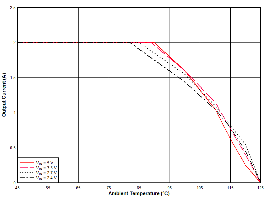
VOUT = 0.6 VTPSM82822RθJA = 64.3°C/W
Figure 9-61 Safe Operating Area
GUID-20200721-CA0I-BGQV-PWGX-BPRCL3CZKNJV-low.gif
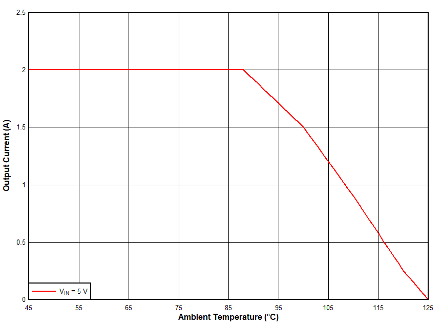
VOUT = 1.8 VTPSM82822RθJA = 64.3°C/W
Figure 9-63 Safe Operating Area
GUID-20200721-CA0I-KBNB-FBFV-BVXTZB3SWQDB-low.gif
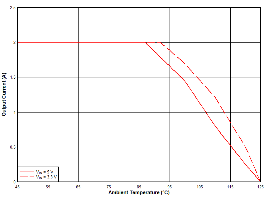
VOUT = 3.3 VTPSM82822RθJA = 64.3°C/W
Figure 9-65 Safe Operating Area
GUID-8353DF32-87D6-4CA8-8B95-52FC46607963-low.gif
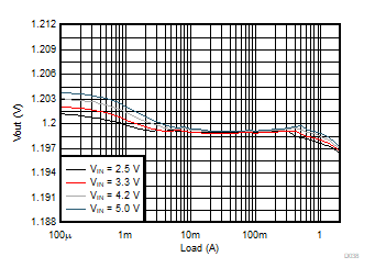
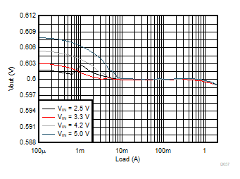
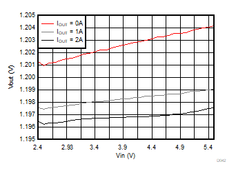
VOUT = 1.2 VTPSM82822
Figure 9-67 Load Regulation
GUID-B8112AEF-697B-47DA-B00C-7E0BFD03F4A5-low.gif
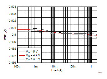
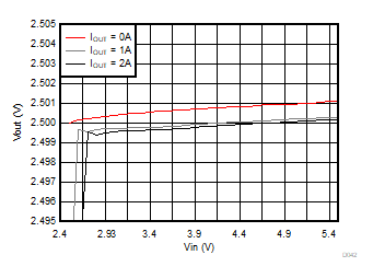
VOUT = 2.5 VTPSM82822
Figure 9-69 Load Regulation
GUID-47E4F2F4-3230-43C1-A6F5-DE7DABA1EF6D-low.gif
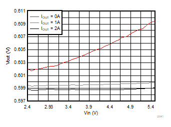
VOUT = 0.6 VTPSM82822
Figure 9-71 Line Regulation
GUID-BC26C2E3-9B8C-4499-9C02-326DE4CFA7D5-low.gif
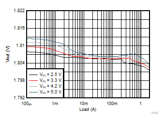
VOUT = 1.8 VTPSM82822
Figure 9-73 Line Regulation
GUID-12490E31-DB3A-4F3E-8EC6-50CBDD75E0D8-low.gif
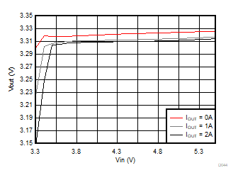
VOUT = 3.3 VTPSM82822
Figure 9-75 Line Regulation
GUID-5734FCC8-EB28-4D4D-96B1-F04C586103F6-low.gif
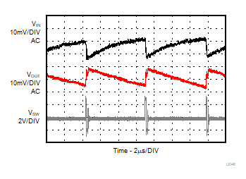
IOUT = 25 mATPSM82822
Figure 9-77 Input and Output Ripple in PSM Mode
GUID-C99C8AA9-8352-4A99-80A3-23262C1362FA-low.gif
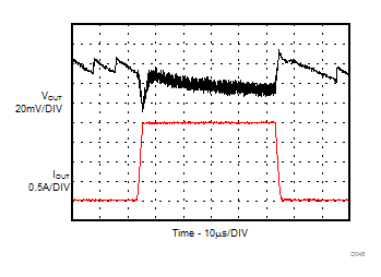
IOUT = 0 A to 2 ASlew Rate = 2 A/µsTPSM82822
Figure 9-79 Load Transient
GUID-7944A088-5545-48B5-B295-05C5CF502026-low.gif
IOUT = no loadTPSM82822
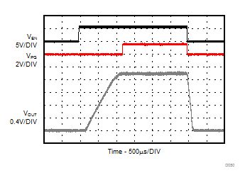
Figure 9-81 Start-up / Shutdown without Load
GUID-2EB5F970-465E-47AA-BA23-755CD0B98C0A-low.gif
TPSM82822
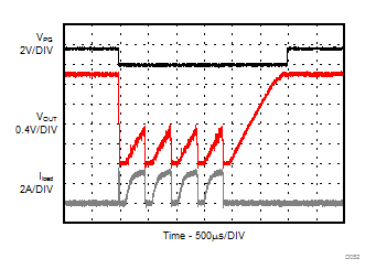
Figure 9-83 Short Circuit, HICCUP Protection Entry / Exit
GUID-2584534C-DD52-4128-B74E-5F3199C1493D-low.gif
TPSM82822
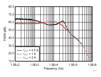
Figure 9-85 Power Supply Rejection Ratio (PSRR)
VIN = 5 VTA = 85°CTPSM82822
Figure 9-54 Efficiency
VIN = 4.2 VTA = 85°CTPSM82822
Figure 9-56 Efficiency
VIN = 3.3 VTA = 85°CTPSM82822
Figure 9-58 Efficiency
VIN = 2.4 VTA = 85°CTPSM82822
Figure 9-60 Efficiency
GUID-20200721-CA0I-5PND-TWT1-T9DBSB1R22KH-low.gif
VOUT = 1.2 VTPSM82822RθJA = 64.3°C/W
Figure 9-62 Safe Operating Area
GUID-20200721-CA0I-DQF1-20JV-X06TTB21V5LV-low.gif
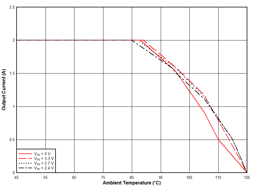
VOUT = 2.5 VTPSM82822RθJA = 64.3°C/W
Figure 9-64 Safe Operating Area
GUID-C627409E-DC4B-4010-BAD9-32CE8ADE9782-low.gif
VOUT = 0.6 VTPSM82822
Figure 9-66 Load Regulation
GUID-EB6CFDF5-9DC3-40CD-8522-13118D5034D9-low.gif
VOUT = 1.8 VTPSM82822
Figure 9-68 Load Regulation
GUID-7E86F950-1F8E-4CF4-B6DD-264E28B02E96-low.gif
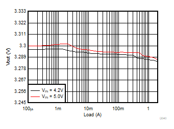
VOUT = 3.3 VTPSM82822
Figure 9-70 Load Regulation
GUID-2D4F8A17-DEB9-4BEC-A9E5-C2F9A7FCBF87-low.gif
VOUT = 1.2 VTPSM82822
Figure 9-72 Line Regulation
GUID-20200626-SS0I-VS7P-790Q-8HD0RQSDZNNV-low.gif
VOUT = 2.5 VTPSM82822
Figure 9-74 Line Regulation
GUID-6696BE22-659C-4834-AA64-61CCCB09A864-low.gif
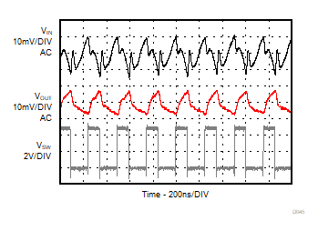
IOUT = 2 ATPSM82822
Figure 9-76 Input and Output Ripple in PWM Mode
GUID-B9CC2AD6-C256-4218-88B8-C02BF7737E5A-low.gif
IOUT = 25 mA to 2 ATPSM82822
Figure 9-78 Load Sweep
GUID-148FA8A6-7BAB-4129-ADD0-7AAB6696F3B0-low.gif
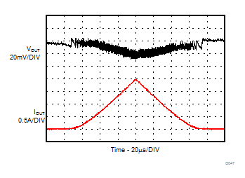
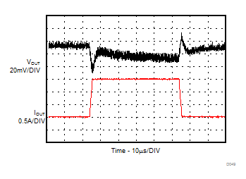
IOUT = 0.5 A to 2 ASlew Rate = 2 A/µsTPSM82822
Figure 9-80 Load Transient
GUID-8732CF3D-F5E9-4F82-9808-E64859A2DD71-low.gif
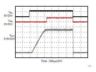
IOUT = 2 ATPSM82822
Figure 9-82 Start-up / Shutdown with Resistive Load
RLOAD = 1 Ω, VIN = 5.5 V (battery supply), VOUT = 1.8 V, tested on TPSM82822EVM-080
Figure 9-84 TPSM82822 Radiated Emissions