ZHCSHU5A July   2017  – March 2018 TPSM82480

PRODUCTION DATA.  

  1. 选项
  2. 应用
  3. 说明
    1.     Device Images
      1.      典型应用电路原理图 空白
      2.      效率与输出电流间的关系空白空白
  4. 修订历史记录
  5. Pin Configuration and Functions
    1.     Pin Functions
  6. Specifications
    1. 6.1 Absolute Maximum Ratings
    2. 6.2 ESD Ratings
    3. 6.3 Recommended Operating Conditions
    4. 6.4 Thermal Information
    5. 6.5 Electrical Characteristics
    6. 6.6 Typical Characteristics
  7. Detailed Description
    1. 7.1 Overview
    2. 7.2 Functional Block Diagram
    3. 7.3 Feature Description
      1. 7.3.1  Enable / Shutdown (EN)
      2. 7.3.2  Soft Start (SS), Pre-biased Output
      3. 7.3.3  Tracking (TR)
      4. 7.3.4  Output Voltage Select (VSEL)
      5. 7.3.5  Forced PWM (MODE)
      6. 7.3.6  Power Good (PG)
      7. 7.3.7  Thermal Good (TG)
      8. 7.3.8  Active Output Discharge
      9. 7.3.9  Undervoltage Lockout (UVLO)
      10. 7.3.10 Thermal Shutdown
    4. 7.4 Device Functional Modes
      1. 7.4.1 Pulse Width Modulation (PWM) Operation
      2. 7.4.2 Power Save Mode (PSM) Operation
      3. 7.4.3 Minimum Duty Cycle and 100% Mode Operation
      4. 7.4.4 Phase Shifted Operation
      5. 7.4.5 Phase Add/Shed and Current Balancing
      6. 7.4.6 Current Limit and Short Circuit Protection
  8. Application and Implementation
    1. 8.1 Application Information
    2. 8.2 Typical Application
      1. 8.2.1 Design Requirements
      2. 8.2.2 Detailed Design Procedure
        1. 8.2.2.1 Setting the Adjustable Output Voltage
        2. 8.2.2.2 Setting VOUT2 Using the VSEL Feature
        3. 8.2.2.3 Output Capacitor Selection
        4. 8.2.2.4 Input Capacitor Selection
        5. 8.2.2.5 Soft Start Capacitor Selection
        6. 8.2.2.6 Tracking
        7. 8.2.2.7 Thermal Good
      3. 8.2.3 Application Curves
    3. 8.3 System Examples
  9. Power Supply Recommendations
  10. 10Layout
    1. 10.1 Layout Guidelines
    2. 10.2 Layout Example
  11. 11器件和文档支持
    1. 11.1 文档支持
      1. 11.1.1 相关文档
    2. 11.2 接收文档更新通知
    3. 11.3 社区资源
    4. 11.4 商标
    5. 11.5 静电放电警告
    6. 11.6 Glossary
  12. 12机械、封装和可订购信息

封装选项

机械数据 (封装 | 引脚)
散热焊盘机械数据 (封装 | 引脚)
订购信息

Application Curves

VIN= 3.6 V, VOUT = 1.8V (R1 / R2 = 240 kΩ / 120 kΩ), TA = 25°C, (unless otherwise noted)
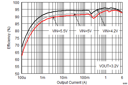
TPSM82480 SLVSDT1_eff32_iout.gif
VOUT = 3.2 V
Figure 10. Efficiency vs Output Current
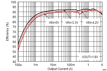
TPSM82480 SLVSDT1_eff18_iout.gif
VOUT = 1.8 V
Figure 12. Efficiency vs Output Current
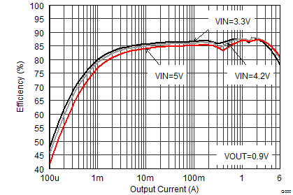
TPSM82480 SLVSDT1_eff09_iout.gif
VOUT = 0.9 V
Figure 14. Efficiency vs Output Current
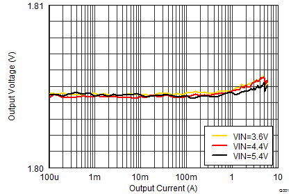
TPSM82480 SLVSCL9_loadreg.gif
Figure 16. Output Voltage vs Output Current
(Load Regulation)
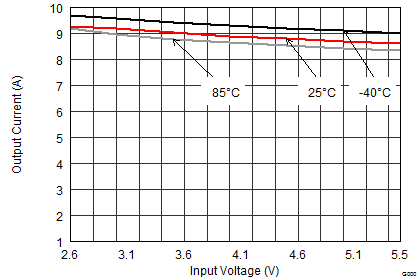
TPSM82480 SLVSCL9_IOUTmax_0.6V.gif
VOUT = 0.6 V
Figure 18. Maximum Output Current
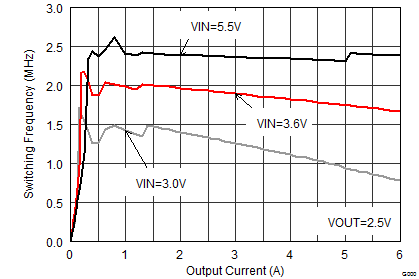
TPSM82480 SLVSCL9_FSWiout2.5V_lin.gif
VOUT = 2.5 V
Figure 20. Switching Frequency vs Output Current
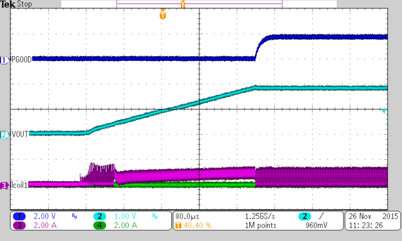
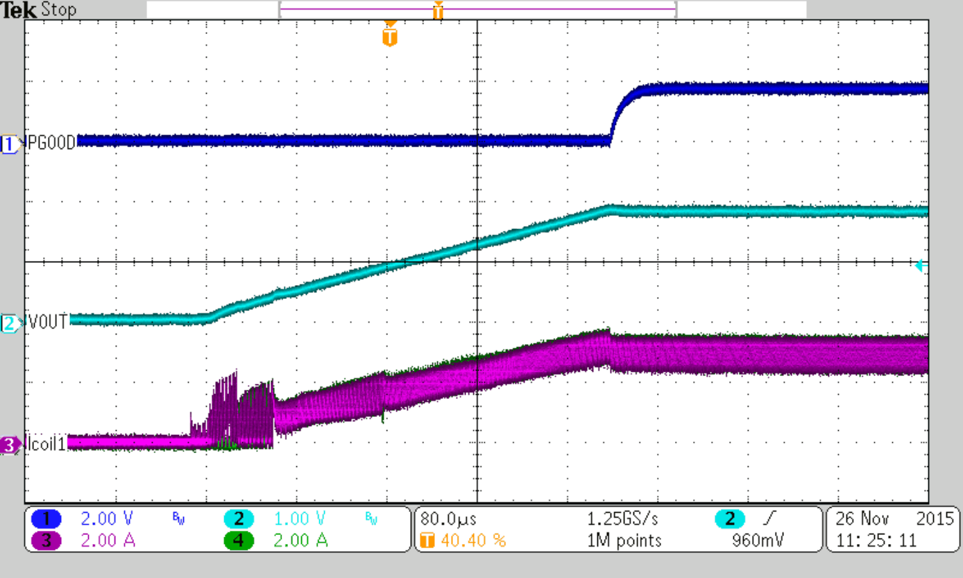
TPSM82480 SLVSCL9_stuplow.gif
VOUT = 1.8 V
Figure 22. Startup into 3.3 Ω resistor
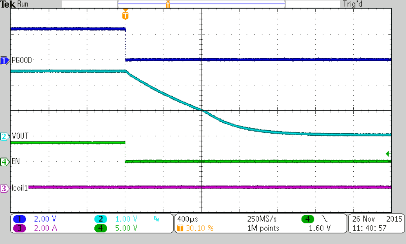
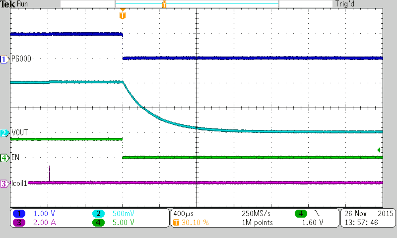
TPSM82480 SLVSCL9_discharge2.5V.gif
VOUT = 2.5 V no load
Figure 24. Output Discharge
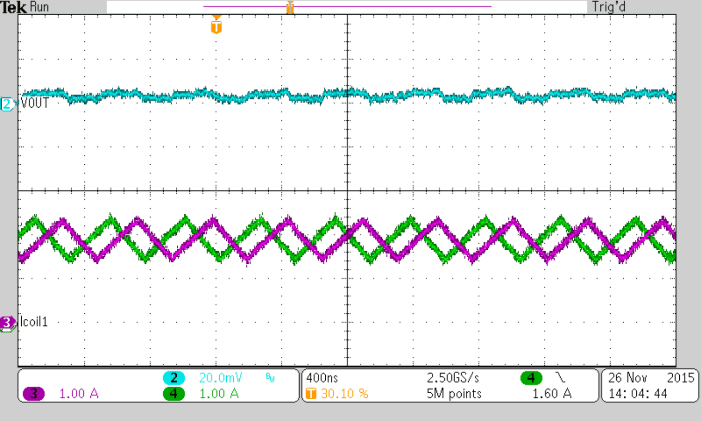
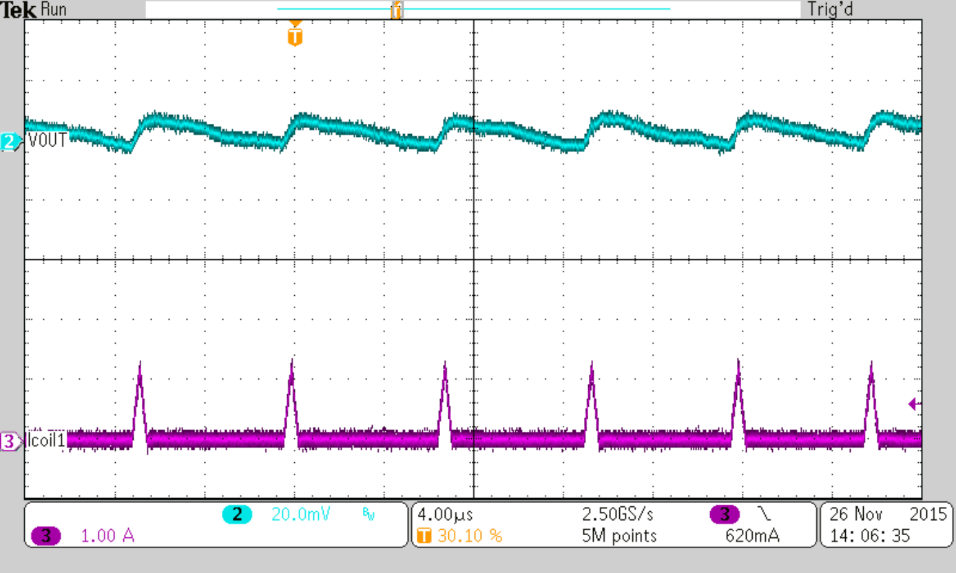
TPSM82480 SLVSCL9_PWMtyp.gif
Figure 26. Typical Operation PWM
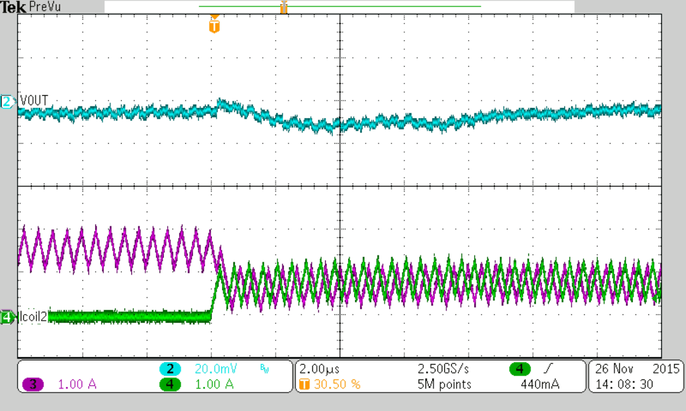
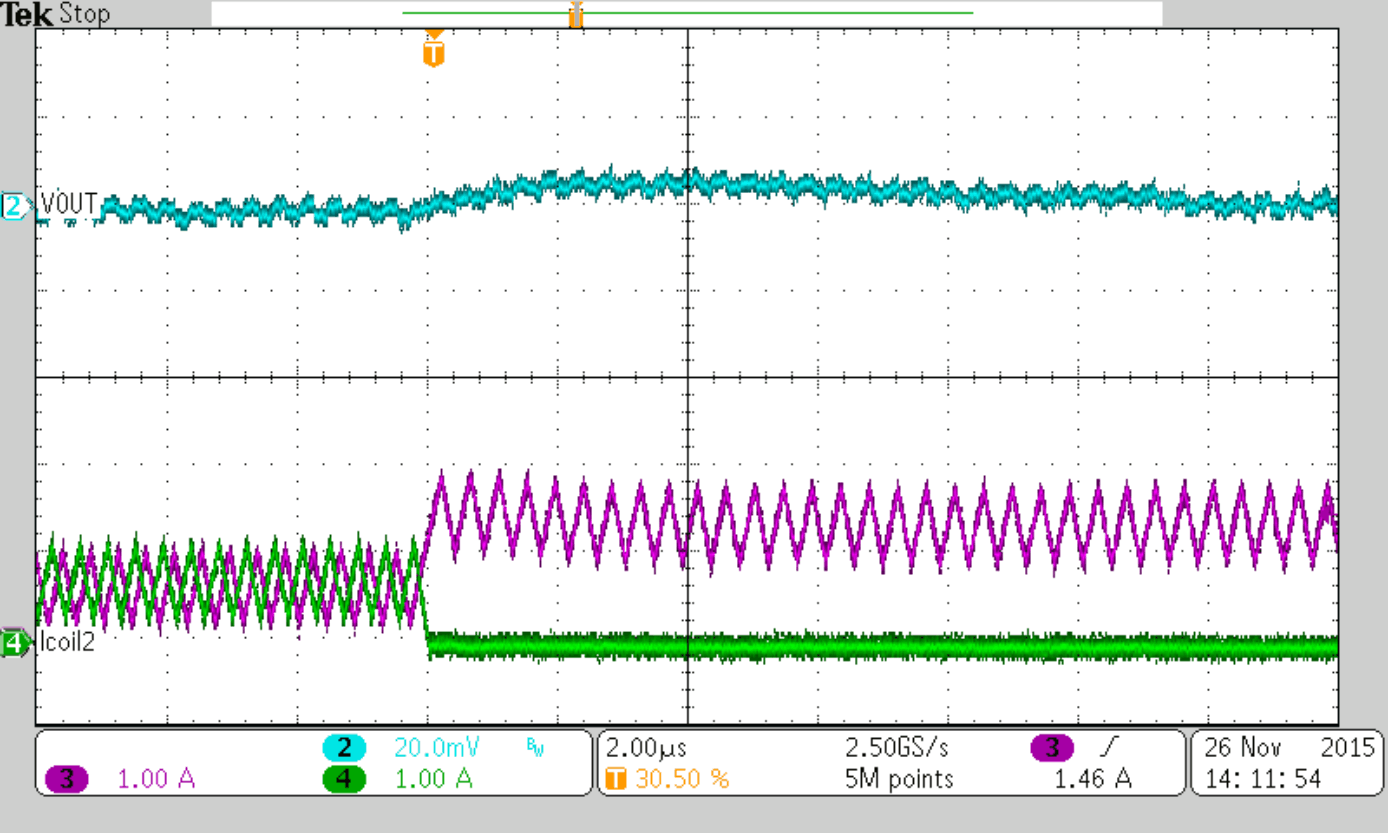
TPSM82480 SLVSCL9_ADD2nd.gif
Figure 28. Adding 2nd Phase
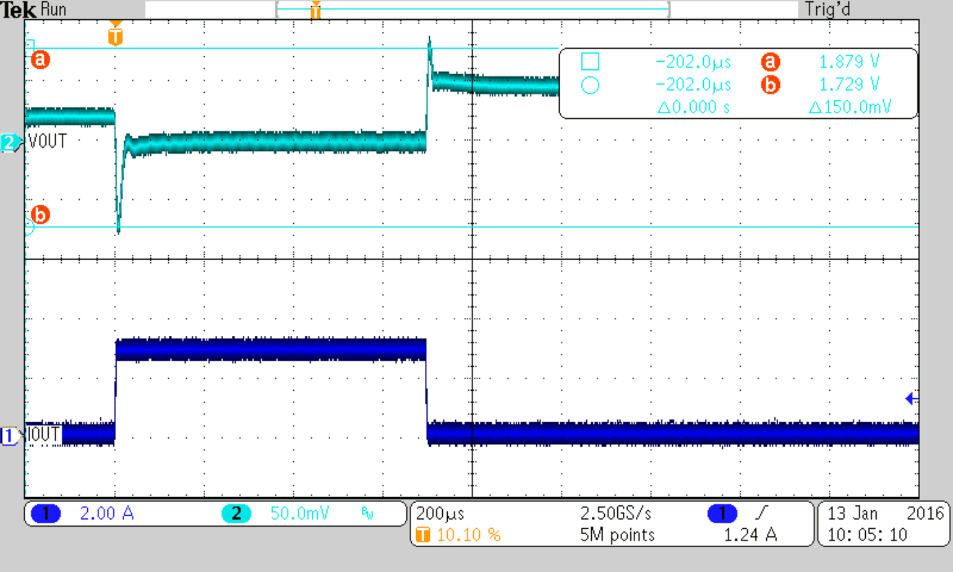
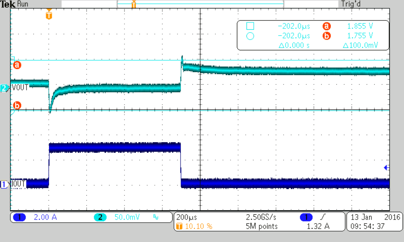
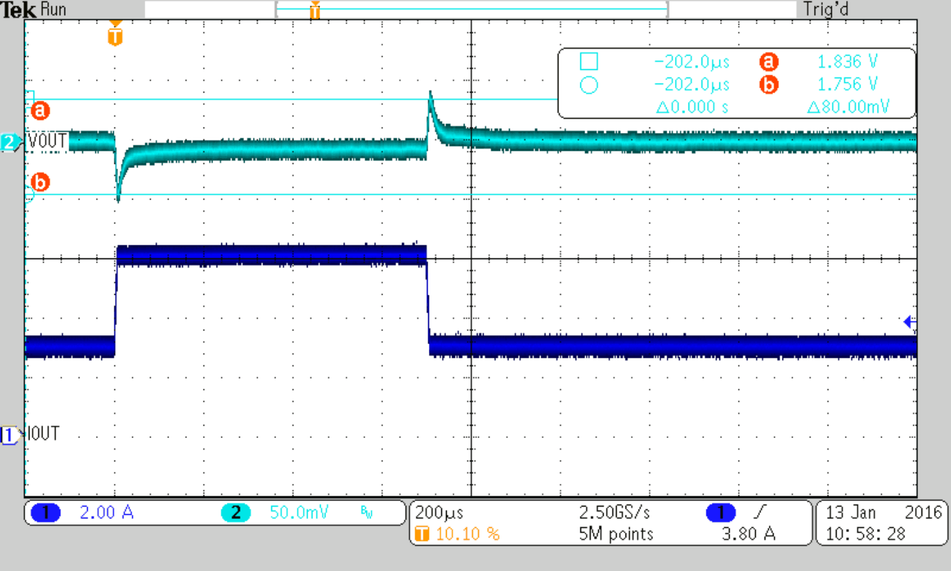
TPSM82480 SLVSCL9_tran_0-3.gif
Figure 30. Load Transient Response (PSM-PWM),
Load Step 0 to 3 A
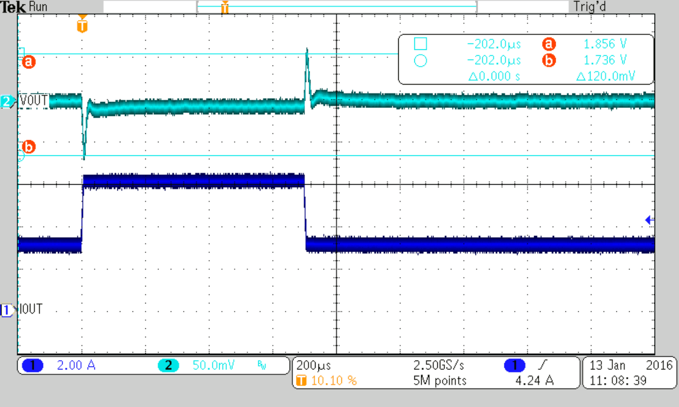
TPSM82480 SLVSCL9_tran_3-6.gif
Figure 32. Load Transient Response (PWM-PWM),
Load Step 3 to 6 A
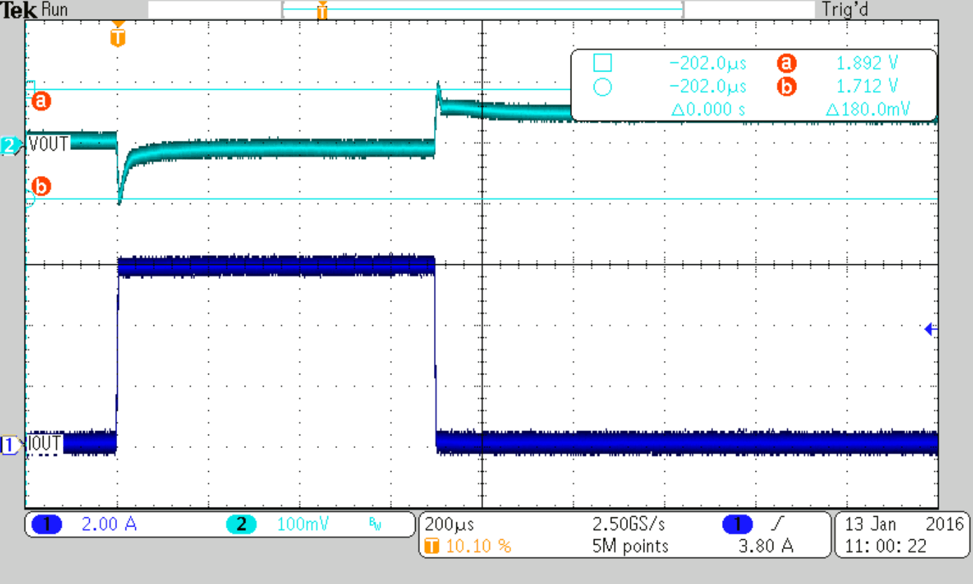
TPSM82480 SLVSCL9_tran_0-6cff.gif
Cff = 36 pF (nom)
Figure 34. Load Transient Response (PWM-PWM),
Load Step 0 to 6 A
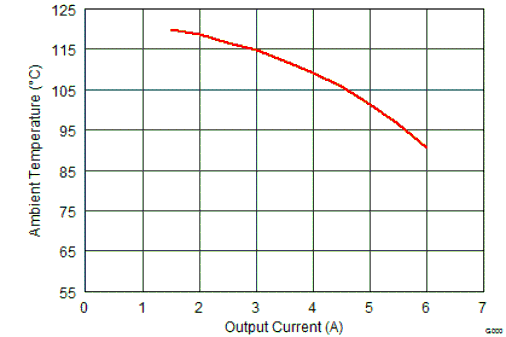
TPSM82480 SLVSDT1_SOA33.gif
VIN = 5 V VOUT = 3.3 V
Figure 36. Maximum Ambient Temperature for TJ=125°C
(TPSM82480 EVM)
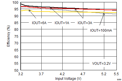
TPSM82480 SLVSDT1_eff32_vin.gif
VOUT = 3.2 V
Figure 11. Efficiency vs Input Voltage
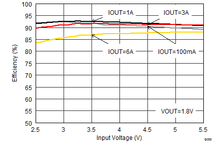
TPSM82480 SLVSDT1_eff18_vin.gif
VOUT = 1.8 V
Figure 13. Efficiency vs Output Voltage
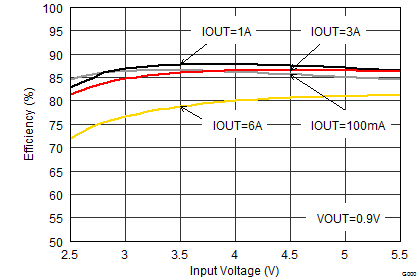
TPSM82480 SLVSDT1_eff09_vin.gif
VOUT = 0.9 V
Figure 15. Efficiency vs Input Voltage
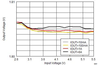
TPSM82480 SLVSCL9_linereg.gif
Figure 17. Output Voltage vs Input Voltage
(Line Regulation)
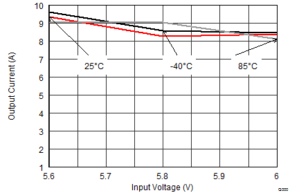
TPSM82480 SLVSCL9_IOUTmax_5.5V.gif
VOUT = 5.5 V
Figure 19. Maximum Output Current
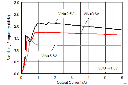
TPSM82480 SLVSCL9_FSWiout1.0V_lin.gif
VOUT = 1 V
Figure 21. Switching Frequency vs Output Current
TPSM82480 SLVSCL9_stuphigh.gif
VOUT = 1.8 V
Figure 23. Startup into 0.3 Ω resistor
TPSM82480 SLVSCL9_discharge1.0V.gif
VOUT = 1 V no load
Figure 25. Output Discharge
TPSM82480 SLVSCL9_PSMtyp.gif
IOUT = 50 mA
Figure 27. Typical Operation PSM
TPSM82480 SLVSCL9_SHED2nd.gif
Figure 29. Shedding 2nd Phase
TPSM82480 SLVSCL9_tran_0-3cff.gif
Cff = 36 pF (nom)
Figure 31. Load Transient Response (PSM-PWM),
Load Step 0 to 3 A
TPSM82480 SLVSCL9_tran_3-6cff.gif
Cff = 36 pF (nom)
Figure 33. Load Transient Response (PWM-PWM),
Load Step 3 to 6 A
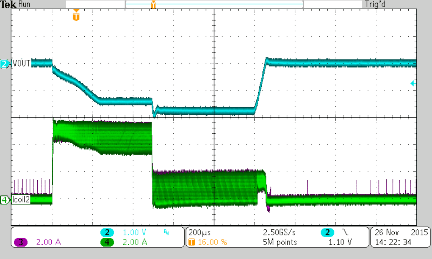
TPSM82480 SLVSCL9_climfoldback.gif
IOUT = 10 A
Figure 35. Current Limit Fold-Back at Overload
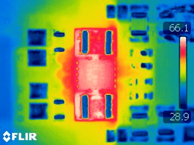
TPSM82480 SLVSDT1_thermal33.gif
VIN = 5 V VOUT = 3.3 V IOUT = 6 A
Figure 37. Device Temperature (TPSM82480 EVM)