ZHCSFD3A April 2016 – August 2016 TPS92515 , TPS92515-Q1 , TPS92515HV , TPS92515HV-Q1
PRODUCTION DATA.
- 1 特性
- 2 应用
- 3 说明
- 4 修订历史记录
- 5 Device Comparison Table
- 6 Pin Configuration and Functions
- 7 Specifications
-
8 Detailed Description
- 8.1 Overview
- 8.2 Functional Block Diagram
- 8.3
Feature Description
- 8.3.1 General Operation
- 8.3.2 Current Sense Comparator
- 8.3.3 OFF Timer
- 8.3.4 OFF-Timer, Shunt FET Dimming or Shunted Output Condition
- 8.3.5 Internal N-channel MOSFET
- 8.3.6 VCC Internal Regulator and Undervoltage Lockout (UVLO)
- 8.3.7 Analog Adjust Input
- 8.3.8 Thermal Protection
- 8.3.9 Junction Temperature Relative Estimation
- 8.3.10 BOOT and BOOT UVLO
- 8.3.11 PWM (UVLO and Enable)
- 8.4 Device Functional Modes
-
9 Application and Implementation
- 9.1 Application Information
- 9.2
Typical Application
- 9.2.1 General Design Procedure
- 9.2.2 Design Requirements
- 9.2.3
Detailed Design Procedure
- 9.2.3.1 Calculating Duty Cycle
- 9.2.3.2 Calculate OFF-Time Estimate
- 9.2.3.3 Calculate OFF-Time Resistor ROFF
- 9.2.3.4 Calculate the Inductance Value
- 9.2.3.5 Calculate the Sense Resistance
- 9.2.3.6 Calculate Input Capacitance
- 9.2.3.7 Verify Peak Current for Inductor Selection
- 9.2.3.8 Calculate Output Capacitance
- 9.2.3.9 Calculate UVLO Resistance Values
- 9.2.4 Application Curves
- 9.3 Dos and Don'ts
- 10Power Supply Recommendations
- 11Layout
- 12器件和文档支持
- 13机械、封装和可订购信息
9 Application and Implementation
NOTE
Information in the following applications sections is not part of the TI component specification, and TI does not warrant its accuracy or completeness. TI’s customers are responsible for determining suitability of components for their purposes. Customers should validate and test their design implementation to confirm system functionality.
9.1 Application Information
The TPS92515 buck current regulator is suitable for implementing step-down LED drivers. This section presents a simplified design process for an LED driver with the following specifications:
- Buck converter topology
- Input voltage: 65 V
- Output voltage: 22 V (7 LEDs)
- Output current 1 A
Use the following design procedure to select component values for this and similar buck applications.
9.2 Typical Application
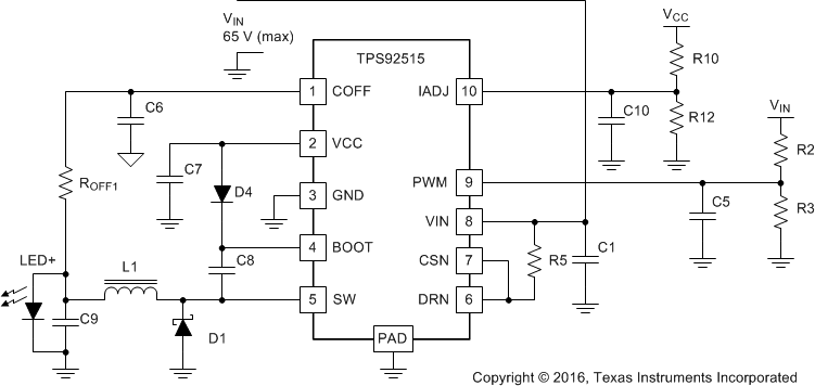 Figure 30. TPS92515 BUCK LED Driver
9.2.1 General Design Procedure
This procedure includes the fundamental design equations required for a TPS92515 buck converter design.
9.2.1.1 Calculating Duty Cycle
Start with an efficiency of n estimation of 0.9.

where
- VOUT = VLED
9.2.1.2 Calculate OFF-Time Estimate
Equation 16 uses the switching period T to derive the OFF-time (tOFF) .

where
- T = [tOFF + tON ]= [tOFF+ (D × T)] and
- T = 1/fSW
9.2.1.3 Calculate OFF-Time Resistor ROFF
Select a COFF between 100 pF and 1 nF. The preferred value is 470 pF. The EC table specifies the OFF-time threshold (VOFT) at 1 V.

9.2.1.4 Calculate the Minimum Inductance Value
Where ΔIL-PP is in Amperes. For example, a 1-A solution with 20% inductor ripple: set ΔIL-PP = 0.2A

When selecting the inductor, ensure the ratings for both peak and average current are adequate. Equation 19 calculates the peak inductor current.

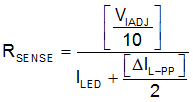
9.2.1.5 Calculate the Sense Resistance
Always use the highest VIADJ voltage the application allows without exceeding 5.5 V. The device clamps any higher value to a level 2.4 V. See also the Analog Adjust Input for details.
9.2.1.6 Calculate Input Capacitance
NOTE
Input voltage ripple (ΔVIN-PP) must not exceed 10% of the input voltage (VIN) or 2 V, whichever is lower.
For example, VIN = 50 V, 50 x 0.1 = 5 V; the maximum ΔVIN-PP remains 2 V.

9.2.1.7 Calculate Output Capacitance
Because current is being regulated and is continuous, no output capacitance is required to supply the load and maintain output voltage. This regulation helps when designing a high-frequency PWM dimming on the LED load. When no output capacitor is used, the same design calculations for ΔIL-PP also apply to ΔILED-PP.
A capacitor placed in parallel with the LED load can be used to reduce ΔILED-PP while keeping the same average current through both the inductor and the LED load. With an output capacitor, the inductance can be lowered, making the magnetic smaller and less expensive. Alternatively, the circuit can be run at lower frequency with the same inductor value, improving the efficiency and increasing the maximum allowable average output voltage. A parallel output capacitor is also useful in applications where the inductor or input voltage tolerance is poor. Adding a capacitor that reduces ΔILED-PP to well below the target provides headroom for changes in inductance or VIN that might otherwise push the maximum ΔILED-PP too high.
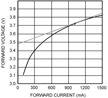 Figure 31. Calculating Dynamic Resistance rD from LED Characteristics.
Determine the output capacitance by establishing the desired ΔILED-PP and the LED dynamic resistance, rD. Calculate the dynamic resistance as the slope of the LED exponential DC characteristic at the nominal operating point as shown in Figure 31. Simply dividing the forward voltage by the forward current at the nominal operating point results in an incorrect value that is between 5 times and 10 times too high. Calculate total dynamic resistance for a string of n LEDs connected in series as the dynamic resistance of one device multiplied by n. Use Equation 22 and Equation 23 to estimate ΔILED-PP when using a parallel capacitor:


9.2.2 Design Requirements
Table 3 shows the design parameters for an example Buck LED driver application.
Table 3. Design Parameters
| PARAMETER | TEST CONDITIONS | MIN | TYP | MAX | UNIT | |
|---|---|---|---|---|---|---|
| INPUT CHARACTERISTICS | ||||||
| VIN | Input voltage range | 30 | 65 | 65 | V | |
| VULVO | Input UVLO setting | 29 | V | |||
| VUVLO-HYST | Input UVLO hysteresis | 4 | ||||
| OUTPUT CHARACTERISTICS | ||||||
| VFLED | LED forward voltage | 3.14159 | V | |||
| n | Number of LEDs in series | 7 | ||||
| VLED | Output voltage | LED+ to LED– | 22 | V | ||
| ILED | Output current | 1000 | mA | |||
| PMAX | Maximum output power | 22 | 25 | W | ||
| SYSTEMS CHARACTERISTICS | ||||||
| ΔILEDpk-pk | LED current ripple | 10% | ||||
| ΔILpk-pk | Inductor current ripple | 45% | ||||
| ΔVIN-PP | Input voltage ripple | 2 | V | |||
| fSW | Switching frequency | 580 | kHz | |||
9.2.3 Detailed Design Procedure
This procedure describes the fundamental component selections for the design specifications noted in Equation 17.
9.2.3.1 Calculating Duty Cycle
Solve for D: VOUT = VLED. Assume a target efficiency of 90%. (η = 0.9)

9.2.3.2 Calculate OFF-Time Estimate
Equation 25 uses the switching period T to derive the OFF-time (tOFF) .

where
- T = tOFF+ tON
- tOFF+ (D x T), and T = 1/fSW
9.2.3.3 Calculate OFF-Time Resistor ROFF
Select a COFF between 100 pF and 1 nF. The preferred value is 470 pF. The EC table specifies the OFF-time threshold (VOFT) at 1 V.

9.2.3.4 Calculate the Inductance Value
this example uses a 1-A solution with 45% inductor ripple. Set ΔIL-PP = 0.45A

where
- ΔIL-PP is in A
When selecting an inductor ensure the ratings for both peak and average current are adequate. Typically an inductance value of at least the calculated value or higher would be selected. For example, most cases use 56 µH or 68 µH given the 52 µH calculation. However, in this example size and efficiency are a concern and the application allows for the use of an output capacitor. Because a value of 52 µH not close to any common values, and output capacitance is allowed, 47 µH is selected. 47 µH has a lower winding resistance (DCR) for the same case size.
9.2.3.5 Calculate the Sense Resistance
Always use the highest VIADJ voltage that the application allows. Do not exceed 5.5 V. A value higher than 2.4 V is clamped to 2.4 V. Refer back to Analog Adjust Input for details.

9.2.3.6 Calculate Input Capacitance
NOTE
Inductor ripple current (ΔVIN-PP) must not exceed 10% of the input voltage (VIN) or 2 V, whichever is lower.
For example, VIN = 65 V, 65 x 0.1 = 6.5 V; the maximum ΔVIN-PP remains 2 V.

9.2.3.7 Verify Peak Current for Inductor Selection
When selecting in inductor consider these three specifications.
- the required inductance
- the average current rating
- the peak current rating
Equation 30calculates the peak current rating

9.2.3.8 Calculate Output Capacitance
 Figure 32. Calculating Dynamic Resistance rDfrom LED Specifications
Solve for rD, using the slope of the tangent line, then multiply by the number of LEDs.

Substitute the value of rD with other parameters to solve for the required minimum output capacitor to meet the required LED ripple current level:

9.2.3.9 Calculate UVLO Resistance Values
Consider the rising threshold of VIN to be 29 V and the hysteresis to be 4 V, calculate R2 and R3 to create the desired operation:


The final schematic is shown in Figure 33 and performance curves in Application Curves:
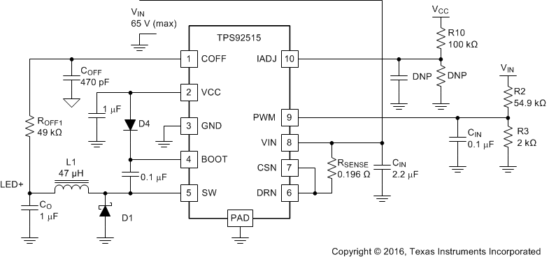 Figure 33. Application Schematic
9.2.4 Application Curves
Buck LED driver example: VOUT = 22 V (7 LEDs), IOUT = 1 A
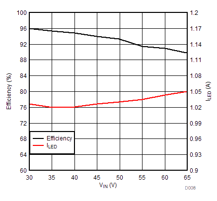
| VLED = 22 V | IOUT = 1.0 A |
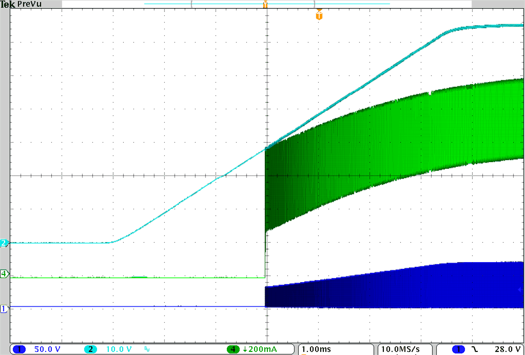
Ch4: Inductor current; UVLO designed limit attained.
Time: 1 ms/div
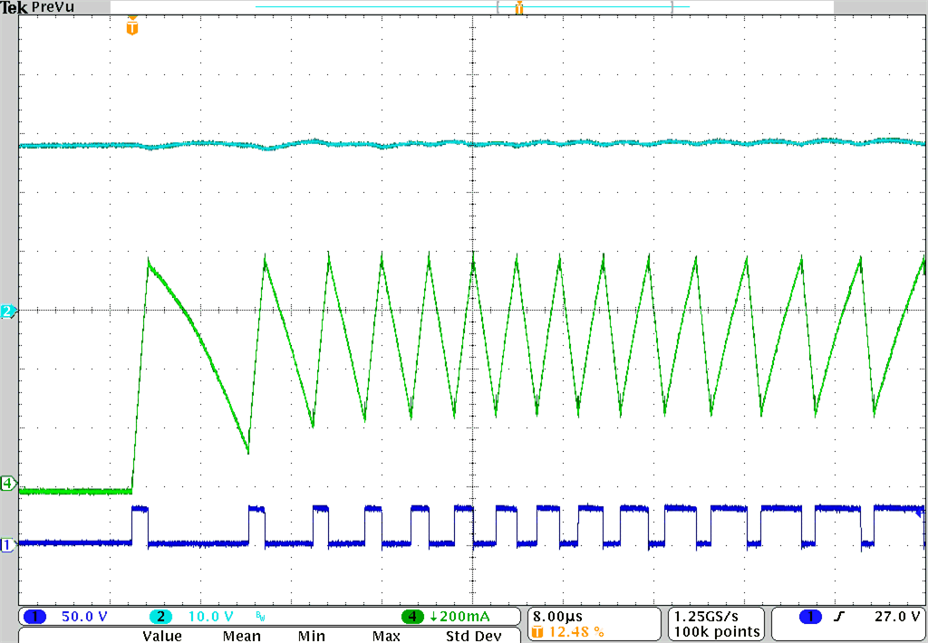
Ch4: Inductor current;
Time: 8 µs/div
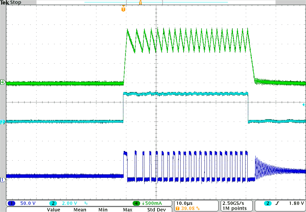
Ch4: Inductor current;
Time: 10 µs/div
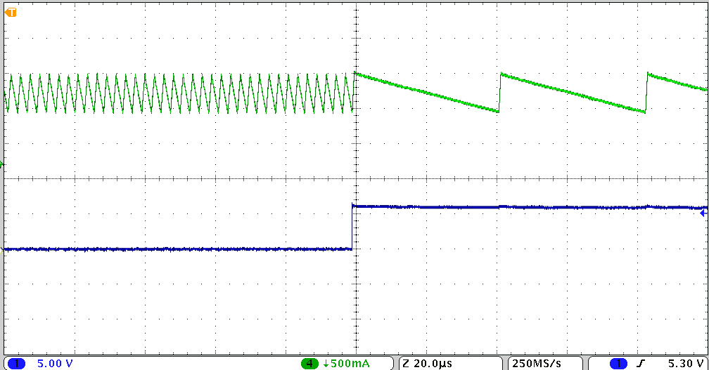
Ch4: Inductor current; ΔIL-PP Maintained
Time: 20 µs/div
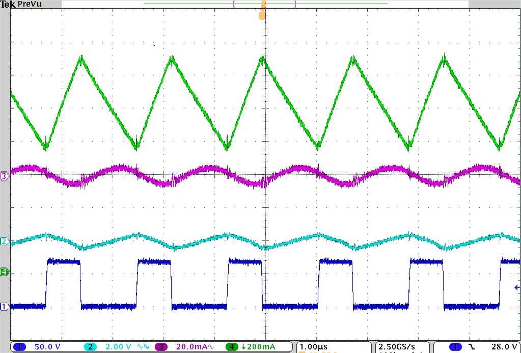
Ch3: ILED-PP; Ch4: Inductor current;
Time: 1 µs/div
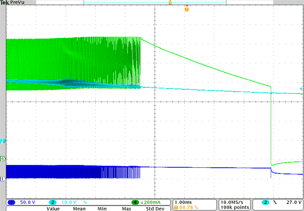
Ch4: Inductor current; UVLO designed limit attained.
Time: 1 ms/div
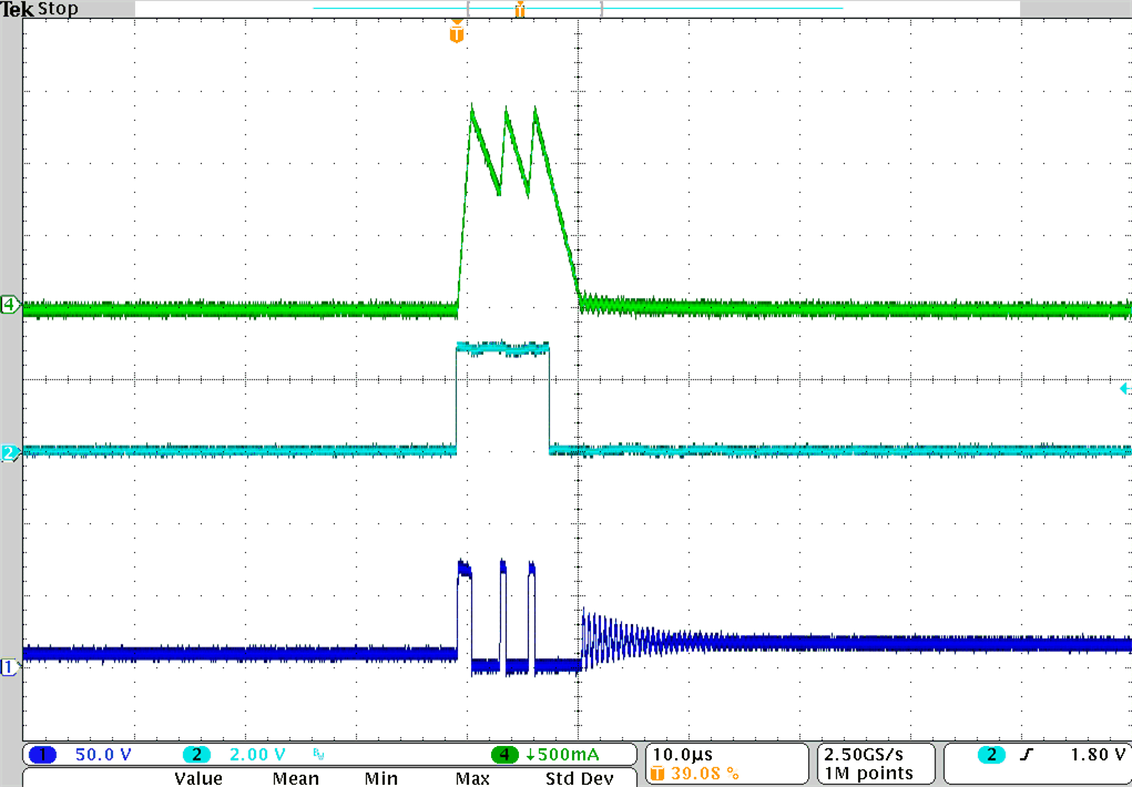
Ch4: Inductor current;
Time: 10 µs/div
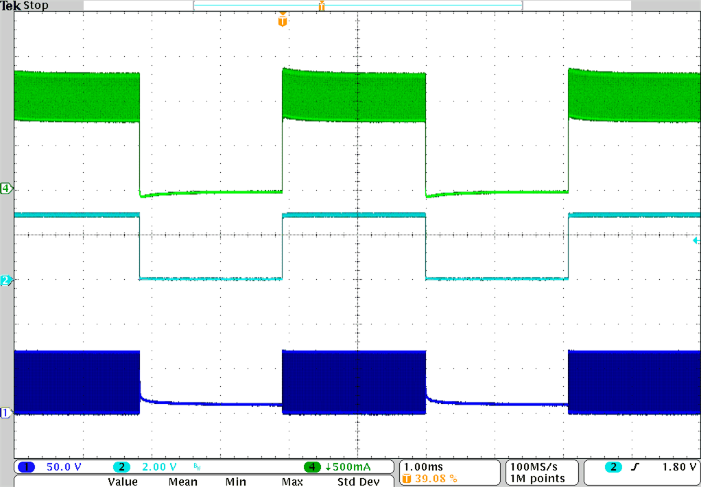
Ch4: Inductor current;
Time: 1 ms/div
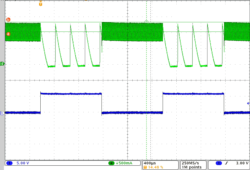
Ch4: Inductor current; OFF-time reaching Maximum OFF-Time
Time: 400 µs/div
9.3 Dos and Don'ts
| Dos | Don'ts |
|---|---|
| Check soldering of thermal pad in production | |
| Check device case and junction temperature during and after prototyping of any solution. |