ZHCSDQ2C January 2015 – September 2018 TPS7B7701-Q1 , TPS7B7702-Q1
PRODUCTION DATA.
- 1 特性
- 2 应用
- 3 说明
- 4 修订历史记录
- 5 Pin Configuration and Functions
- 6 Specifications
-
7 Detailed Description
- 7.1 Overview
- 7.2 Functional Block Diagram
- 7.3
Feature Description
- 7.3.1 Fault Detection and Protection
- 7.3.2 Short-Circuit and Overcurrent Protection
- 7.3.3 Short-to-Battery and Reverse Current Detection
- 7.3.4 Thermal Shutdown
- 7.3.5 Integrated Reverse-Polarity Protection
- 7.3.6 Integrated Inductive Clamp
- 7.3.7 Undervoltage Lockout
- 7.3.8 Enable (EN, EN1, and EN2)
- 7.3.9 Internal Voltage Regulator (VCC)
- 7.3.10 Current Sense Multiplexing
- 7.3.11 Adjustable Output Voltage (FB, FB1, and FB2)
- 7.4 Device Functional Modes
- 8 Application and Implementation
- 9 Power Supply Recommendations
- 10Layout
- 11器件和文档支持
- 12机械、封装和可订购信息
7.3.11 Adjustable Output Voltage (FB, FB1, and FB2)
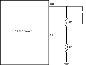
Using an external resistor divider selects an output voltage between 1.5 V and 20 V. Use Table 2 to calculate the output voltage (VO). The recommended value for both R1 and R2 is less than 100 kΩ.
Equation 1. 

where
- V(FB) = 1.233 V
 Figure 21. TPS7B770x-Q1 Output Voltage Setting Connection
 The TPS7B770x-Q1 family of devices can also be used as a current-limited switch by connecting the FB pin to the GND pin.