ZHCSPJ2A December 2021 – May 2022 TPS7A13
PRODUCTION DATA
- 1 特性
- 2 应用
- 3 说明
- 4 Revision History
- 5 Pin Configuration and Functions
- 6 Specifications
- 7 Detailed Description
-
8 Application and Implementation
- 8.1
Application Information
- 8.1.1 Recommended Capacitor Types
- 8.1.2 Input, Output, and Bias Capacitor Requirements
- 8.1.3 Dropout Voltage
- 8.1.4 Behavior During Transition From Dropout Into Regulation
- 8.1.5 Device Enable Sequencing Requirement
- 8.1.6 Load Transient Response
- 8.1.7 Undervoltage Lockout Circuit Operation
- 8.1.8 Power Dissipation (PD)
- 8.1.9 Estimating Junction Temperature
- 8.1.10 Recommended Area for Continuous Operation
- 8.2 Typical Application
- 8.1
Application Information
- 9 Power Supply Recommendations
- 10Layout
- 11Device and Documentation Support
- 12Mechanical, Packaging, and Orderable Information
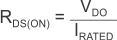
8.1.3 Dropout Voltage
Dropout voltage (VDO) is defined as the input voltage minus the output voltage (VIN – VOUT) at the rated output current (IRATED), where the pass transistor is fully on. IRATED is the maximum IOUT listed in the Section 6.3 table. The pass transistor is in the ohmic or triode region of operation, and acts as a switch. The dropout voltage indirectly specifies a minimum input voltage greater than the nominal programmed output voltage at which the output voltage is expected to stay in regulation. If the input voltage falls to less than the nominal output regulation, then the output voltage falls as well.
For a CMOS regulator, the dropout voltage is determined by the drain-source on-state resistance (RDS(ON)) of the pass transistor. Therefore, if the linear regulator operates at less than the rated current, the dropout voltage for that current scales accordingly. Use Equation 1 to calculate the RDS(ON) of the device.
Using a bias rail enables the TPS7A13 to achieve a lower dropout voltage between IN and OUT. However, a minimum bias voltage above the nominal programmed output voltage must be maintained. Figure 6-13 specifies the minimum VBIAS headroom required to maintain output regulation.