SBVS128F June 2009 – December 2015 TPS727
PRODUCTION DATA.
- 1 Features
- 2 Applications
- 3 Description
- 4 Revision History
- 5 Pin Configurations and Functions
- 6 Specifications
- 7 Detailed Description
- 8 Applications and Implementation
- 9 Power-Supply Recommendations
- 10Layout
- 11Device and Documentation Support
- 12Mechanical, Packaging, and Orderable Information
封装选项
请参考 PDF 数据表获取器件具体的封装图。
机械数据 (封装 | 引脚)
- YFF|4
- DSE|6
散热焊盘机械数据 (封装 | 引脚)
订购信息
10 Layout
10.1 Layout Guidelines
10.1.1 Board Layout Recommendations to Improve PSRR and Noise Performance
To improve ac performance (such as PSRR, output noise, and transient response), TI recommends that the board be designed with separate ground planes for VIN and VOUT, with the ground plane connected only at the GND pin of the device. In addition, the ground connection for the output capacitor must be connected directly to the GND pin of the device. High ESR capacitors may degrade PSRR.
10.1.2 Power Dissipation
The ability to remove heat from the die is different for each package type, presenting different considerations in the printed circuit board (PCB) layout. The PCB area around the device that is free of other components moves the heat from the device to the ambient air. Performance data for JEDEC low- and high-K boards are given in the Thermal Information table. Using heavier copper increases the effectiveness in removing heat from the device. The addition of plated through-holes to heat-dissipating layers also improves the heatsink effectiveness.
Power dissipation depends on input voltage and load conditions. Power dissipation (PD) is equal to the product of the output current times the voltage drop across the output pass element (VIN to VOUT), as shown in Equation 3:

10.2 Layout Example
10.2.1 DSE EVM Board Layout
This section provides the TPS727xxDSEEVM-406 board layout and illustrations.
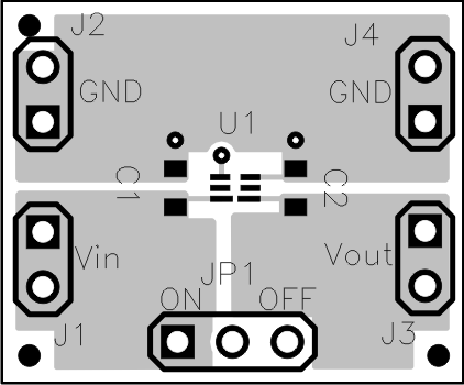 Figure 36. Top Layer Assembly
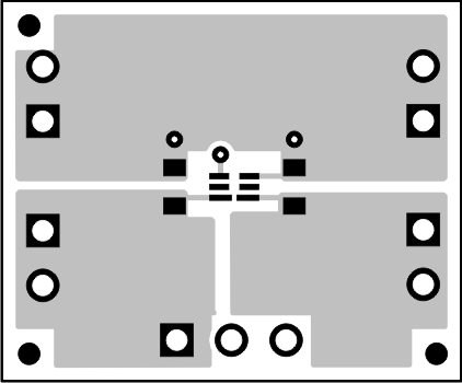 Figure 37. Top Layer Routing
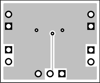 Figure 38. Bottom Layer Routing
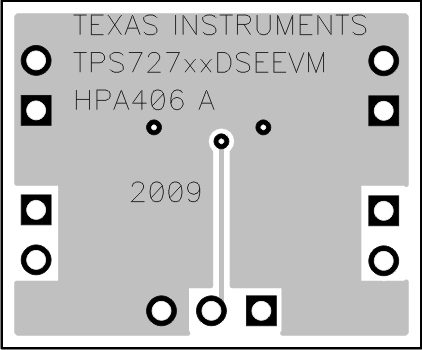 Figure 39. Bottom Layer Assembly
10.2.2 YFF EVM Board Layout
This section provides the TPS727xxYFFEVM-407 board layout and illustrations.
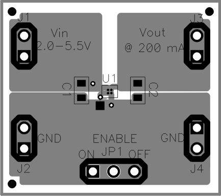 Figure 40. Top Layer Assembly
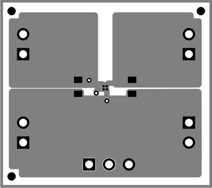 Figure 41. Top Layer Routing
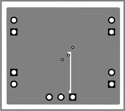 Figure 42. Bottom Layer Routing
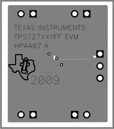 Figure 43. Bottom Layer Assembly