SBVS100E June   2008  – September 2015 TPS720

PRODUCTION DATA.  

  1. Features
  2. Applications
  3. Description
    1.     Simplified Schematic
  4. Revision History
  5. Pin Configuration and Functions
    1.     Pin Functions
  6. Specifications
    1. 6.1 Absolute Maximum Ratings
    2. 6.2 ESD Ratings
    3. 6.3 Recommended Operating Conditions
    4. 6.4 Thermal Information
    5. 6.5 Electrical Characteristics
    6. 6.6 Typical Characteristics
  7. Detailed Description
    1. 7.1 Overview
    2. 7.2 Functional Block Diagram
    3. 7.3 Feature Description
      1. 7.3.1 Internal Current Limit
      2. 7.3.2 Inrush Current Limit
      3. 7.3.3 Shutdown
      4. 7.3.4 Undervoltage Lockout (UVLO)
    4. 7.4 Device Functional Modes
  8. Application and Implementation
    1. 8.1 Application Information
      1. 8.1.1 Input and Output Capacitor Requirements
      2. 8.1.2 Output Regulation With IN Pin Floating
      3. 8.1.3 Dropout Voltage
      4. 8.1.4 Transient Response
      5. 8.1.5 Minimum Load
    2. 8.2 Typical Application
      1. 8.2.1 Design Requirements
      2. 8.2.2 Detailed Design Procedures
      3. 8.2.3 Application Curves
  9. Power Supply Recommendations
  10. 10Layout
    1. 10.1 Layout Guidelines
    2. 10.2 Layout Example
    3. 10.3 Thermal Considerations
    4. 10.4 Power Dissipation
  11. 11Device and Documentation Support
    1. 11.1 Device Support
      1. 11.1.1 Development Support
        1. 11.1.1.1 Evaluation Module
      2. 11.1.2 Device Nomenclature
    2. 11.2 Documentation Support
      1. 11.2.1 Related Documentation
    3. 11.3 Community Resources
    4. 11.4 Trademarks
    5. 11.5 Electrostatic Discharge Caution
    6. 11.6 Glossary
  12. 12Mechanical, Packaging, and Orderable Information
    1. 12.1 Package Mounting

封装选项

机械数据 (封装 | 引脚)
散热焊盘机械数据 (封装 | 引脚)
订购信息

Application Curves

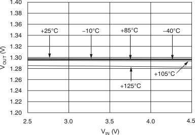
TPS720 tc_line_vin_350_bvs100.gif
IOUT = 350 mA
Figure 29. VIN Line Regulation (TPS72013YZU)
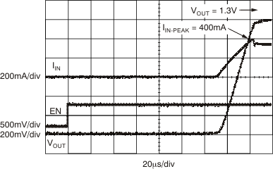
TPS720 tc_inrush_350ma_bvs100.gif
VIN = 1.8 V VOUT = 1.3 V VBIAS = 2.7 V
IOUT = 350 mA
Figure 31. VIN Inrush Current
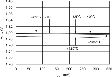
TPS720 tc_load_reg_bvs100.gif
Figure 30. Load Regulation (TPS72013YZU)
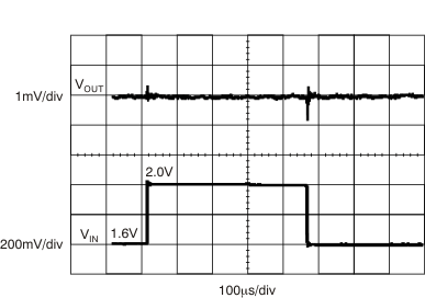
TPS720 tc_line_resp_vin_bvs100.gif
VIN = 1.6 to 2 V VOUT = 1.3 V VBIAS = 2.7 V
VIN Slew Rate = 1 V/μs IOUT = 350 mA
Figure 32. VIN Line Transient Response