ZHCSLZ8A September   2020  – August 2021 TPS65988DK

PRODUCTION DATA  

  1. 特性
  2. 应用
  3. 说明
  4. Revision History
  5. Pin Configuration and Functions
  6. Specifications
    1. 6.1  Absolute Maximum Ratings
    2. 6.2  ESD Ratings
    3. 6.3  Recommended Operating Conditions
    4. 6.4  Thermal Information
    5. 6.5  Power Supply Requirements and Characteristics
    6. 6.6  Power Consumption Characteristics
    7. 6.7  Power Switch Characteristics
    8. 6.8  Cable Detection Characteristics
    9. 6.9  USB-PD Baseband Signal Requirements and Characteristics
    10. 6.10 Thermal Shutdown Characteristics
    11. 6.11 Oscillator Characteristics
    12. 6.12 I/O Characteristics
    13. 6.13 I2C Requirements and Characteristics
    14. 6.14 SPI Controller Timing Requirements
    15. 6.15 HPD Timing Requirements
    16. 6.16 Typical Characteristics
  7. Parameter Measurement Information
  8. Detailed Description
    1. 8.1 Overview
    2. 8.2 Functional Block Diagram
    3. 8.3 Feature Description
      1. 8.3.1  USB-PD Physical Layer
        1. 8.3.1.1 USB-PD Encoding and Signaling
        2. 8.3.1.2 USB-PD Bi-Phase Marked Coding
        3. 8.3.1.3 USB-PD Transmit (TX) and Receive (Rx) Masks
        4. 8.3.1.4 USB-PD BMC Transmitter
        5. 8.3.1.5 USB-PD BMC Receiver
      2. 8.3.2  Power Management
        1. 8.3.2.1 Power-On and Supervisory Functions
        2. 8.3.2.2 VBUS LDO
        3. 8.3.2.3 Supply Switch Over
      3. 8.3.3  Port Power Switches
        1. 8.3.3.1 PP_HV Power Switch
          1. 8.3.3.1.1 PP_HV Overcurrent Clamp
          2. 8.3.3.1.2 PP_HV Overcurrent Protection
          3. 8.3.3.1.3 PP_HV OVP and UVP
          4. 8.3.3.1.4 PP_HV Reverse Current Protection
        2. 8.3.3.2 Schottky for Current Surge Protection
        3. 8.3.3.3 PP_EXT Power Path Control
        4. 8.3.3.4 PP_CABLE Power Switch
          1. 8.3.3.4.1 PP_CABLE Overcurrent Protection
          2. 8.3.3.4.2 PP_CABLE Input Good Monitor
        5. 8.3.3.5 VBUS Transition to VSAFE5V
        6. 8.3.3.6 VBUS Transition to VSAFE0V
      4. 8.3.4  Cable Plug and Orientation Detection
        1. 8.3.4.1 Configured as a DFP
        2. 8.3.4.2 Configured as a UFP
        3. 8.3.4.3 Configured as a DRP
        4. 8.3.4.4 Fast Role Swap Signaling
      5. 8.3.5  Dead Battery Operation
        1. 8.3.5.1 Dead Battery Advertisement
        2. 8.3.5.2 BUSPOWER (ADCIN1)
      6. 8.3.6  ADC
      7. 8.3.7  DisplayPort HPD
      8. 8.3.8  Digital Interfaces
        1. 8.3.8.1 General GPIO
        2. 8.3.8.2 I2C
        3. 8.3.8.3 SPI
      9. 8.3.9  Digital Core
      10. 8.3.10 I2C Interfaces
        1. 8.3.10.1 I2C Interface Description
        2. 8.3.10.2 I2C Clock Stretching
        3. 8.3.10.3 I2C Address Setting
        4. 8.3.10.4 Unique Address Interface
        5. 8.3.10.5 I2C Pin Address Setting (ADCIN2)
      11. 8.3.11 SPI Controller Interface
      12. 8.3.12 Thermal Shutdown
      13. 8.3.13 Oscillators
    4. 8.4 Device Functional Modes
      1. 8.4.1 Boot
      2. 8.4.2 Power States
  9. Application and Implementation
    1. 9.1 Application Information
    2. 9.2 Typical Applications
      1. 9.2.1 USB4 Device Application with Host Charging
        1. 9.2.1.1 Design Requirements
          1. 9.2.1.1.1 Power Supply Design Requirements
        2. 9.2.1.2 Detailed Design Procedure
          1. 9.2.1.2.1 USB Power Delivery Source Capabilities
          2. 9.2.1.2.2 USB Power Delivery Sink Capabilities
          3. 9.2.1.2.3 Supported Data Modes
          4. 9.2.1.2.4 USB4 Hub Controller & PD Controller I2C Communication
          5. 9.2.1.2.5 Dock Management Controller & PD Controller I2C Communication
          6. 9.2.1.2.6 SPI Flash Options
  10. 10Power Supply Recommendations
    1. 10.1 3.3-V Power
      1. 10.1.1 VIN_3V3 Input Switch
      2. 10.1.2 VBUS 3.3-V LDO
    2. 10.2 1.8-V Power
    3. 10.3 Recommended Supply Load Capacitance
  11. 11Layout
    1. 11.1  Layout Guidelines
    2. 11.2  Layout Example
    3. 11.3  Stack-up and Design Rules
    4. 11.4  Main Component Placement
    5. 11.5  Super Speed Type-C Connectors
    6. 11.6  Capacitor Placement
    7. 11.7  CC1/2 Capacitors & ADCIN1/2 Resistors
    8. 11.8  CC and SBU Protection Placement
    9. 11.9  CC Routing
    10. 11.10 DRAIN1 and DRAIN2 Pad Pours
    11. 11.11 VBUS Routing
    12. 11.12 Completed Layout
    13. 11.13 Power Dissipation
  12. 12Device and Documentation Support
    1. 12.1 Device Support
      1. 12.1.1 Firmware Warranty Disclaimer
    2. 12.2 Documentation Support
      1. 12.2.1 Related Documentation
    3. 12.3 支持资源
    4. 12.4 Trademarks
    5. 12.5 Electrostatic Discharge Caution
    6. 12.6 术语表
  13. 13Mechanical, Packaging, and Orderable Information

封装选项

机械数据 (封装 | 引脚)
散热焊盘机械数据 (封装 | 引脚)
订购信息

Super Speed Type-C Connectors

In this layout example a dual row SMT mid mount Type-C connector is used. Start by placing vias for all the signals on the Type-C connector that need to be routed on another layer. Once the vias have been placed, route out the super speed lines and place their ESD protection close to the Type-C connector. The figures below show the via placement, top routing, and bottom routing for the super speed signals on the Type-C connector. The same should be implemented for both Type-C connectors.
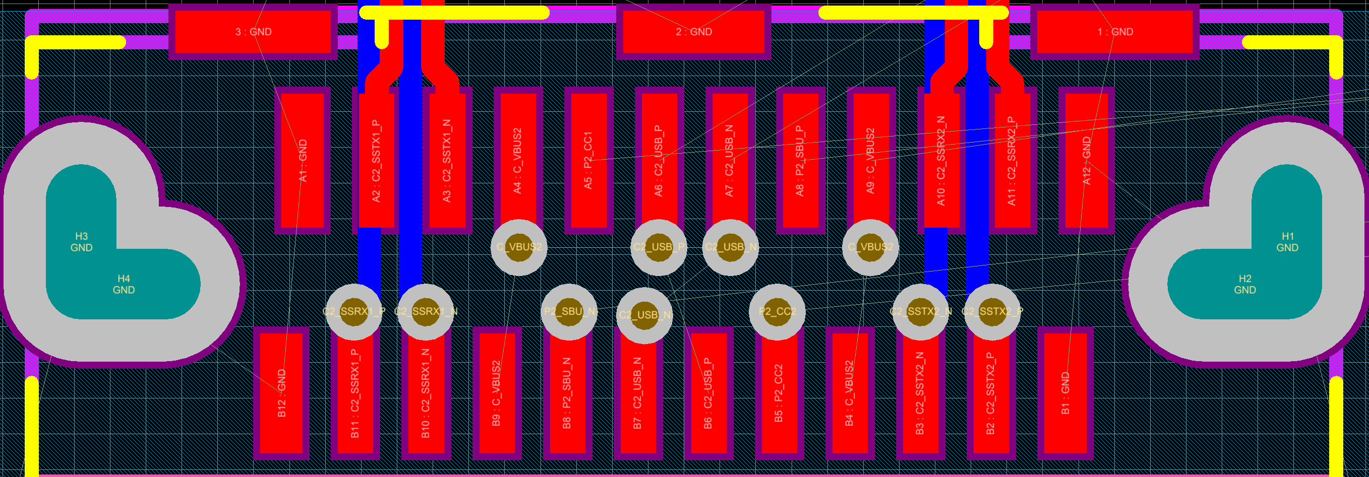
GUID-430B4B36-7B8F-4057-BBB2-341E9F416C37-low.pngFigure 11-6 Type-C Connector Via Placement
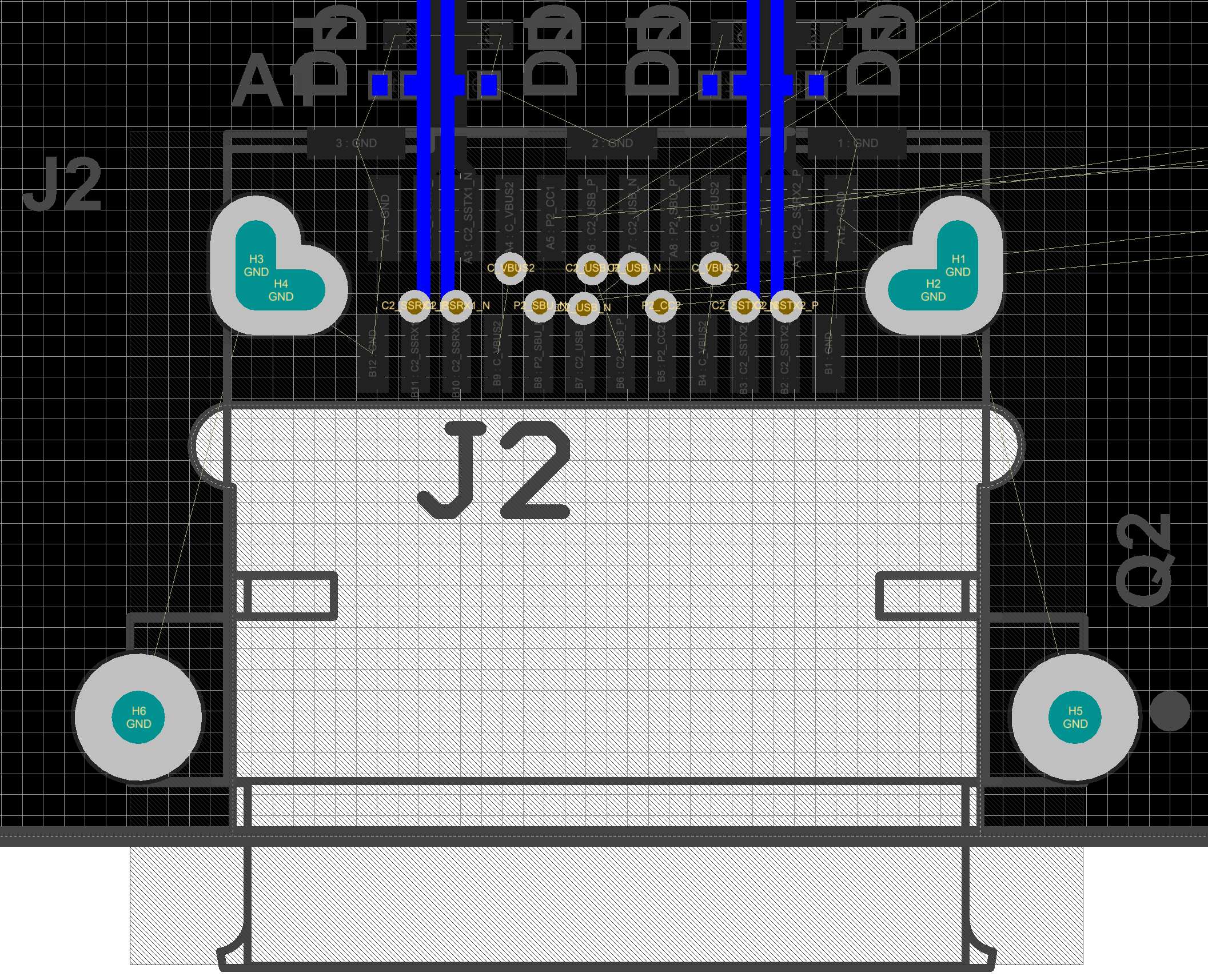
GUID-C1405CD7-F85E-42DB-A6BF-FEACFE6FC1EA-low.pngFigure 11-8 Type-C Connector SSTXRX Bottom Layer
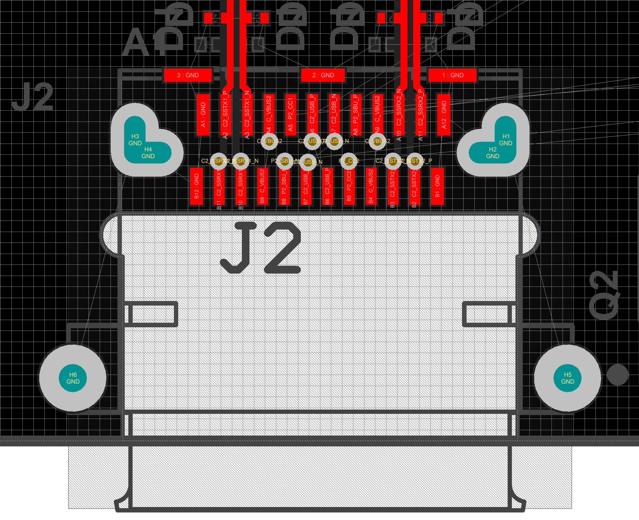
GUID-1F4DD657-3709-4482-BD47-58B8D9954E0F-low.pngFigure 11-7 Type-C Connector SSTXRX Top Layer