ZHCSDG2 March 2015 TPS65632
PRODUCTION DATA.
- 1 特性
- 2 应用范围
- 3 说明
- 4 简化电路原理图
- 5 修订历史记录
- 6 Pin Configuration and Functions
- 7 Specifications
-
8 Detailed Description
- 8.1 Overview
- 8.2 Functional Block Diagram
- 8.3 Feature Description
- 8.4 Device Functional Modes
- 9 Application and Implementation
- 10Power Supply Recommendations
- 11Layout
- 12器件和文档支持
- 13机械、封装和可订购信息
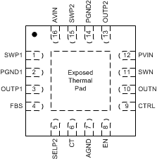
6 Pin Configuration and Functions
RTE Package
16-Pin WQFN with Thermal Pad
Top View

Pin Functions
| PIN | TYPE(1) | DESCRIPTION | ||
|---|---|---|---|---|
| NAME | NO. | |||
| AGND | 7 | GND | Analog ground. | |
| AVIN | 16 | PWR | Supply voltage for the device. | |
| CT | 6 | I/O | A capacitor connected between this pin and ground sets the transition time for VNEG when programmed to a new value. | |
| CTRL | 9 | I | Boost converter 1 (VPOS) inverting buck-boost converter (VNEG) enable/program. | |
| EN | 8 | I | Boost converter 2 (AVDD) enable. | |
| FBS | 4 | I | Boost converter 1 (VPOS) sense input. | |
| OUTN | 10 | O | Inverting buck-boost converter output (VNEG). | |
| OUTP | 3 | O | Boost converter 1 output (VPOS). | |
| OUTP2 | 13 | O | Boost converter 2 output (AVDD). | |
| PGND1 | 2 | GND | Boost converter 1 power ground. | |
| PGND2 | 14 | GND | Boost converter 2 power ground. | |
| PVIN | 12 | PWR | Inverting buck-boost converter power stage supply voltage. | |
| SELP2 | 5 | I | Boost converter 2 output voltage selection pin. AVDD = 7.7 V when SELP2 = low and 5.8 V when SELP2 = high. | |
| SWN | 11 | I/O | Inverting buck-boost converter switch pin. | |
| SWP1 | 1 | I | Boost converter 1 switch pin. | |
| SWP2 | 15 | I | Boost converter 2 switch pin. | |
| Exposed thermal pad | — | Connect this pad to AGND, PGND1 and PGND2. | ||
(1) GND = Ground, PWR = Power, I = Input, O = Output, I/O = Input/Output