ZHCSJF4 February 2019 TPS65295
PRODUCTION DATA.
- 1 特性
- 2 应用
- 3 说明
- 4 修订历史记录
- 5 Pin Configuration and Functions
- 6 Specifications
- 7 Detailed Description
- 8 Application and Implementation
- 9 Power Supply Recommendations
- 10Layout
- 11器件和文档支持
- 12机械、封装和可订购信息
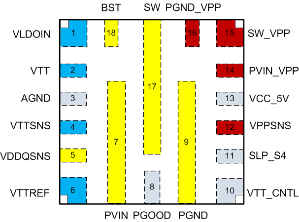
5 Pin Configuration and Functions
RJE Package
18-Pin VQFN
Top View

Pin Functions
| PIN | I/O | DESCRIPTION | |
|---|---|---|---|
| NAME | NO. | ||
| VLDOIN | 1 | P | Power supply input for VTT LDO. Connect VDDQ in typical application. |
| VTT | 2 | O | VTT 1-A LDO output. Recommend to connect to 10-μF or larger capacitance for stability. |
| AGND | 3 | G | Signal ground. |
| VTTSNS | 4 | I | VTT output voltage feedback. |
| VDDQSNS | 5 | I | VDDQ output voltage feedback. |
| VTTREF | 6 | O | Buffered VTT reference output. Recommend to connect to 0.22-μF or larger capacitance for stability. |
| PVIN | 7 | P | Input power supply for VDDQ buck. |
| PGOOD | 8 | O | Power good signal open-drain output. PGOOD goes high when VPP and VDDQ output voltage are within the target range. |
| PGND | 9 | G | Power ground for VDDQ buck. |
| VTT_CNTL | 10 | I | VTT_CNTL signal input for VTT LDO enable control. For detail control setup, please refer toTable 1. |
| SLP_S4 | 11 | I | SLP_S4 signal input for VDDQ buck and VPP buck enable control. For detail control setup, please refer toTable 1. |
| VPPSNS | 12 | I | VPP output voltage feedback. |
| VCC_5V | 13 | P | Power supply for VPP and VDDQ buck converter control logic circuit. |
| PVIN_VPP | 14 | P | Input power supply for VPP buck. |
| SW_VPP | 15 | O | VPP switching node connection to the inductor and bootstrap capacitor. |
| PGND_VPP | 16 | G | Power ground for VPP buck. |
| SW | 17 | O | VDDQ switching node connection to the inductor and bootstrap capacitor. |
| BST | 18 | I | High-side MOSFET gate driver bootstrap voltage input for VDDQ buck. Connect a capacitor between the BST pin and the SW pin. |