ZHCSEC5D November 2015 – May 2021 TPS65235
PRODUCTION DATA
- 1 特性
- 2 应用
- 3 说明
- 4 Revision History
- 5 Pin Configuration and Functions
- 6 Specifications
-
7 Detailed Description
- 7.1 Overview
- 7.2 Functional Block Diagram
- 7.3
Feature Description
- 7.3.1 Boost Converter
- 7.3.2 Linear Regulator and Current Limit
- 7.3.3 Boost Converter Current Limit
- 7.3.4 Charge Pump
- 7.3.5 Slew Rate Control
- 7.3.6 Short Circuit Protection, Hiccup and Overtemperature Protection
- 7.3.7 Tone Generation
- 7.3.8 Tone Detection
- 7.3.9 Disable and Enable
- 7.3.10 Component Selection
- 7.4 Device Functional Modes
- 7.5 Programming
- 7.6 Register Maps
- 8 Application and Implementation
- 9 Power Supply Recommendations
- 10Layout
- 11Device and Documentation Support
- 12Mechanical, Packaging, and Orderable Information
7.3.10.1 Boost Inductor
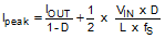
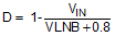
TPS65235 is recommended to operate with a boost inductor value of 4.7 µH or 10 µH. The boost inductor must be able to support the peak current requirement to maintain the maximum LNB output current without saturation. Below formula can be used to estimate the peak current of the boost inductor.
With the different inductance, the system will have different gain and phase margins, Figure 7-5 shows a Bode plot of boost loop with 2 x 10 µF / 35 V of boost capacitor and 4.7 µH, 5.6 µH, 6.8 µH, 8.2 µH and 10 µH of boost inductance. As the boost inductance increases, the 0 dB crossover frequency keeps relatively constant while the phase and gain margins reduced. With 4.7 µH, the phase margin is 66.96° and with 10 µH the phase margin is 39.63°.
") Figure 7-5 Gain and Phase Margin of the Boost Loop with Different Inductance (VIN = 12 V, VOUT = 18.2 V, ILOAD = 1 A, FSW = 1 MHz, 5 µF, Typical Bode Plot)
Figure 7-5 Gain and Phase Margin of the Boost Loop with Different Inductance (VIN = 12 V, VOUT = 18.2 V, ILOAD = 1 A, FSW = 1 MHz, 5 µF, Typical Bode Plot)