ZHCSM97A November 2020 – August 2021 TPS6521845
PRODUCTION DATA
- 1 特性
- 2 应用
- 3 说明
- 4 Revision History
- 5 Pin Configuration and Functions
- 6 Specifications
-
7 Detailed Description
- 7.1 Overview
- 7.2 Functional Block Diagram
- 7.3
Feature Description
- 7.3.1
Wake-Up and Power-Up and Power-Down Sequencing
- 7.3.1.1 Power-Up Sequencing
- 7.3.1.2 Power-Down Sequencing
- 7.3.1.3 Strobe 1 and Strobe 2
- 7.3.1.4 Supply Voltage Supervisor and Power-Good (PGOOD)
- 7.3.1.5 Backup Supply Power-Good (PGOOD_BU)
- 7.3.1.6 Internal LDO (INT_LDO)
- 7.3.1.7 Current Limited Load Switches
- 7.3.1.8 LDO1
- 7.3.1.9 Coin Cell Battery Voltage Acquisition
- 7.3.1.10 UVLO
- 7.3.1.11 Power-Fail Comparator
- 7.3.1.12 Battery-Backup Supply Power-Path
- 7.3.1.13 DCDC3 and DCDC4 Power-Up Default Selection
- 7.3.1.14 I/O Configuration
- 7.3.1.15 Push Button Input (PB)
- 7.3.1.16 AC_DET Input (AC_DET)
- 7.3.1.17 Interrupt Pin (INT)
- 7.3.1.18 I2C Bus Operation
- 7.3.1
Wake-Up and Power-Up and Power-Down Sequencing
- 7.4 Device Functional Modes
- 7.5 Register Maps
- 8 Application and Implementation
- 9 Power Supply Recommendations
- 10Layout
- 11Device and Documentation Support
- 12Mechanical, Packaging, and Orderable Information
7.3.1.11 Power-Fail Comparator
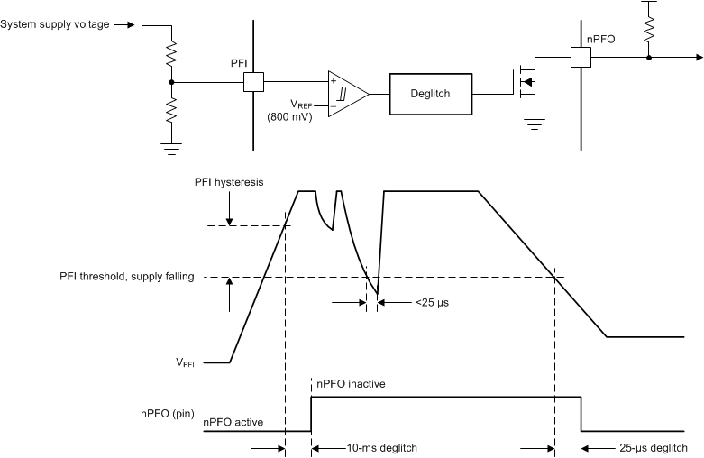
The power-fail comparator notifies the system host if the system supply voltage drops and the system is at risk of shutting down. The comparator has an internal 800-mV threshold and the trip-point is adjusted by an external resistor divider.
By default, the power-fail comparator has no impact on any of the power rails or load switches. Load switches are configured individually, to be disabled when the PFI comparator trips to shed system load and extend hold-up time as described in GUID-AA1520A6-0C74-4283-A9E8-91737DCA8585.html#GUID-AA1520A6-0C74-4283-A9E8-91737DCA8585. The power-fail comparator also triggers the power-down sequencer, such that all or selective rails power-down when the system voltage fails. To tie the power-fail comparator into the power-down sequence, the OFFnPFO bit in the CONTROL register must be set to 1.
The power-fail comparator cannot be monitored by software, such that no interrupt or status bit is associated to this function.
 Figure 7-17 Power-Fail Comparator Simplified Circuit and Timing Diagram