ZHCSIX2 October 2018 TPS65216
PRODUCTION DATA.
- 1器件概述
- 2Pin Configuration and Functions
- 3Specifications
-
4Detailed Description
- 4.1 Overview
- 4.2 Functional Block Diagram
- 4.3
Feature Description
- 4.3.1
Wake-Up and Power-Up and Power-Down Sequencing
- 4.3.1.1 Power-Up Sequencing
- 4.3.1.2 Power-Down Sequencing
- 4.3.1.3 Strobes 1 and 2
- 4.3.1.4 Supply Voltage Supervisor and Power Good (PGOOD)
- 4.3.1.5 Internal LDO (INT_LDO)
- 4.3.1.6 Current Limited Load Switch
- 4.3.1.7 LDO1
- 4.3.1.8 UVLO
- 4.3.1.9 Power-Fail Comparator
- 4.3.1.10 DCDC3 / DCDC4 Power-Up Default Selection
- 4.3.1.11 I/O Configuration
- 4.3.1.12 Push Button Input (PB)
- 4.3.1.13 AC_DET Input (AC_DET)
- 4.3.1.14 Interrupt Pin (INT)
- 4.3.1.15 I2C Bus Operation
- 4.3.1
Wake-Up and Power-Up and Power-Down Sequencing
- 4.4 Device Functional Modes
- 4.5
Register Maps
- 4.5.1 Password Protection
- 4.5.2 FLAG Register
- 4.5.3
TPS65216Registers
- 4.5.3.1 CHIPID Register (subaddress = 0x0) [reset = 0x5]
- 4.5.3.2 INT1 Register (subaddress = 0x1) [reset = 0x0]
- 4.5.3.3 INT2 Register (subaddress = 0x2) [reset = 0x0]
- 4.5.3.4 INT_MASK1 Register (subaddress = 0x3) [reset = 0x0]
- 4.5.3.5 INT_MASK2 Register (subaddress = 0x4) [reset = 0x0]
- 4.5.3.6 STATUS Register (subaddress = 0x5) [reset = 00XXXXXXb]
- 4.5.3.7 CONTROL Register (subaddress = 0x6) [reset = 0x0]
- 4.5.3.8 FLAG Register (subaddress = 0x7) [reset = 0x0]
- 4.5.3.9 PASSWORD Register (subaddress = 0x10) [reset = 0x0]
- 4.5.3.10 ENABLE1 Register (subaddress = 0x11) [reset = 0x0]
- 4.5.3.11 ENABLE2 Register (subaddress = 0x12) [reset = 0x0]
- 4.5.3.12 CONFIG1 Register (subaddress = 0x13) [reset = 0x4C]
- 4.5.3.13 CONFIG2 Register (subaddress = 0x14) [reset = 0xC0]
- 4.5.3.14 CONFIG3 Register (subaddress = 0x15) [reset = 0x0]
- 4.5.3.15 DCDC1 Register (offset = 0x16) [reset = 0x99]
- 4.5.3.16 DCDC2 Register (subaddress = 0x17) [reset = 0x99]
- 4.5.3.17 DCDC3 Register (subaddress = 0x18) [reset = 0x8C]
- 4.5.3.18 DCDC4 Register (subaddress = 0x19) [reset = 0xB2]
- 4.5.3.19 SLEW Register (subaddress = 0x1A) [reset = 0x6]
- 4.5.3.20 LDO1 Register (subaddress = 0x1B) [reset = 0x1F]
- 4.5.3.21 SEQ1 Register (subaddress = 0x20) [reset = 0x0]
- 4.5.3.22 SEQ2 Register (subaddress = 0x21) [reset = 0x0]
- 4.5.3.23 SEQ3 Register (subaddress = 0x22) [reset = 0x98]
- 4.5.3.24 SEQ4 Register (subaddress = 0x23) [reset = 0x75]
- 4.5.3.25 SEQ5 Register (subaddress = 0x24) [reset = 0x12]
- 4.5.3.26 SEQ6 Register (subaddress = 0x25) [reset = 0x63]
- 4.5.3.27 SEQ7 Register (subaddress = 0x26) [reset = 0x3]
- 5Application and Implementation
- 6Power Supply Recommendations
- 7Layout
- 8器件和文档支持
- 9机械、封装和可订购信息
4.3.1.6 Current Limited Load Switch
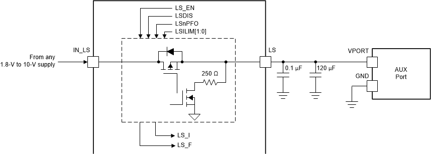
The TPS65216 provides a current limited load switch with individual enable control. The load switch provides the following control and diagnostic features:
- The ON/OFF state of the switch is controlled by the corresponding LS_EN bit in the ENABLE register.
- The load switch can only be controlled through I2C communication. The sequencer has no control over the load switch.
- The load switch has an active discharge function, disabled by default, and enabled through the LSDCHRG bit. When enabled, the switch output is discharged to ground whenever the switch is disabled.
- When the PFI input drops below the power-fail threshold (the power-fail comparator trips), the load switch is automatically disabled to shed system load. This function must be individually through the corresponding LSnPFO bit. The switch does not turn back on automatically as the system voltage recovers, and must be manually re-enabled.
- An interrupt (LS_I) issues whenever the load switch actively limits the output current, such as when the output load exceeds the current limit value. The switch remains ON and provides current to the load according to the current-limit setting.
- The load switch has a local overtemperature sensor which disables the switch if the power dissipation and junction temperature exceeds safe operating value. The switch automatically recovers once the temperature drops below the OTS threshold value minus hysteresis. The LS_F (fault) interrupt bit is set while the switch is held OFF by the OTS function.
The load switch (LS) is a non-reverse blocking, medium-voltage (< 10 V), low-impedance switch that can be used to provide 1.8-V to 10-V power to an auxiliary port. LS has four selectable current limit values that are selectable through LSILIM[1:0].
 Figure 4-10 Typical Application of Load Switch