ZHCS259B July 2011 – August 2015 TPS65142
PRODUCTION DATA.
- 1 特性
- 2 应用
- 3 说明
- 4 修订历史记录
- 5 Pin Configuration and Functions
- 6 Specifications
-
7 Detailed Description
- 7.1 Overview
- 7.2 Functional Block Diagram
- 7.3
Feature Description
- 7.3.1 AVDD Boost Regulator
- 7.3.2 Regulated Positive Charge Pump
- 7.3.3 Negative Charge Pump
- 7.3.4 Gate Voltage Shaping
- 7.3.5 VCOM Buffer
- 7.3.6 Reset
- 7.3.7 Under-voltage Lockout (UVLO)
- 7.3.8 Thermal Shutdown
- 7.3.9 WLED Boost Regulator
- 7.3.10 Current Sinks
- 7.3.11 Unused IFB Pins
- 7.3.12 PWM Dimming
- 7.3.13 Enabling the WLED Driver
- 7.3.14 Soft-Start of WLED Boost Regulator
- 7.3.15 Protection of WLED Driver
- 7.3.16 Power Up/Down Sequence
- 8 Application and Implementation
- 9 器件和文档支持
- 10机械、封装和可订购信息
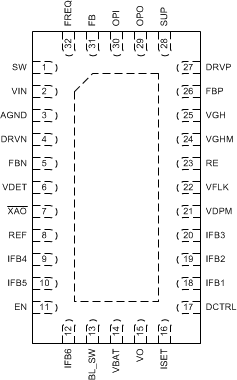
5 Pin Configuration and Functions
WQFN Package
32-Pin (RTG)
Top View

Pin Functions
| PIN | I/O | DESCRIPTION | |
|---|---|---|---|
| NAME | NO. | ||
| AGND | 3 | Analog ground | |
| BL_SW | 13 | The backlight boost converter switching node | |
| DCTRL | 17 | I | Backlight PWM dimming control input |
| DRVN | 4 | O | Voltage driver of the negative charge pump |
| DRVP | 27 | Voltage driver of positive charge pump | |
| EN | 11 | I | Backlight enable input |
| FB | 31 | I | AVDD Boost converter feedback pin |
| FBN | 5 | I | Negative charge pump feedback pin |
| FBP | 26 | I | Positive charge pump feedback pin |
| FREQ | 32 | I | AVDD boost converter switching frequency selection: 1.2MHz when V(FREQ) = VIN and 650 kHz when V(FREQ) = ground |
| IFB1 | 18 | I | Channel 1 of the WLED backlight current sink |
| IFB2 | 19 | I | Channel 2 of the WLED backlight current sink |
| IFB3 | 20 | I | Channel 3 of the WLED backlight current sink |
| IFB4 | 9 | I | Channel 4 of the WLED backlight current sink |
| IFB5 | 10 | I | Channel 5 of the WLED backlight current sink |
| IFB6 | 12 | I | Channel 6 of the WLED backlight current sink |
| ISET | 16 | I | WLED current sink level programming input |
| OPI | 30 | I | Input voltage of VCOM Buffer |
| OPO | 29 | O | Output voltage of VCOM Buffer |
| PGND | ePAD | Exposed pad that serves as the power ground for both boost converters | |
| RE | 23 | Sets the slope for the gate shaping function. Pin for external Resistor | |
| REF | 8 | O | Reference voltage for the negative charge pump |
| SUP | 28 | I | Supply pin of the gate shaping and operational amplifier blocks. Connected as well to the overvoltage protection comparator. This pin needs to be connected to the output of the AVDD boost converter. |
| SW | 1 | Switch pin of the AVDD boost converter | |
| VBAT | 14 | I | Input of the backlight boost converter |
| VDET | 6 | I | Reset IC threshold pin (Voltage divider) |
| VDPM | 21 | O | Sets the delay to enable VGHM Output. Pin for external capacitor. Floating if no delay needed |
| VFLK | 22 | I | Charge/discharge signal for VGHM |
| VGH | 25 | I | Input for positive Charge Pump |
| VGHM | 24 | O | Output for gate-high modulation |
| VIN | 2 | I | Input supply pin |
| VO | 15 | O | The output of the backlight boost converter |
| XAO | 7 | O | Reset IC output pulling down XAO pin when active. |