ZHCSBR7C August 2013 – June 2017 TPS65000-Q1
PRODUCTION DATA.
7 Detailed Description
7.1 Overview
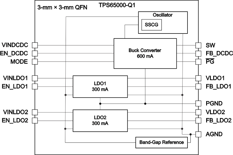
The TPS65000-Q1 device provides one step-down converter, two low dropout regulators and spread spectrum clock generation. The device has an input voltage range of
2.3 V to 6 V. This device is intended for (but not limited to) powering automotive camera modules.
The output voltage of the step-down converter can be selected through resistor networks on the output. To maximize efficiency, there are two modes of operation based on load conditions: PWM or PFM. By pulling the MODE pin high, forced PWM can be achieved. Pulling this pin low results in an automatic adjustment between PFM and PWM modes.
The two general-purpose low-dropout regulators each have their own separate enables and voltage inputs. The inputs can be tied to the output of the step-down converter or to a separate voltage source. Resistor networks are required on the output of the regulator to set the output voltage.
The switching frequency of the step-down converter is handled by the oscillator, with a typical frequency of
2.25 MHz. The spread spectrum clock (SSC) modulates this frequency when the device is in PWM mode. This additional circuit in the oscillator block reduces power that may cause EMI.
The TPS65000-Q1 device also provides a power good signal to monitor the condition of the DC-DC and both LDOs. The DC-DC and LDOs are only monitored if their enable signal is high. If all enabled resources are in regulation, the pin is pulled low. If one or more of the enabled resources are out of regulation, the pin is placed in Hi-Z .
7.2 Functional Block Diagram
7.3 Feature Description
7.3.1 Step-Down Converter
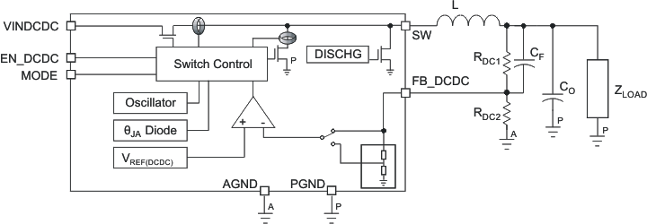
The step-down converter is intended to allow maximum flexibility in the end equipment. The output voltage is user-selectable with a resistor network on the output. Figure 16 shows the necessary connections.
The output voltage of the DC-DC converter is set by Equation 1:
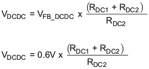
The combined resistance of RDC1 and RDC2 should be less than 1 MΩ.
Fixed output voltages and additional current-limit options are also possible. Contact TI for further information.
The step-down converter has two modes of operation to maximize efficiency at different load conditions. At moderate to heavy load currents, the device operates in a fixed-frequency pulse-width modulation (PWM) mode that results in small output ripple and high efficiency. Pulling the MODE pin to a DC-high level results in PWM mode over the entire load range.
At light load currents, the device operates in a pulsed frequency-modulation (PFM) mode to improve efficiency. The transition to this mode occurs when the inductor current through the low-side FET becomes zero, indicating discontinuous conduction. PFM mode also results in the output voltage increasing by 1% from its nominally set value. This voltage positioning is intended to minimize both the voltage undershoot of a load step from light to heavy loads, as when a processor moves from sleep to active modes, and the voltage overshoot at load removal. Figure 17 shows the voltage positioning behavior for a light-to-heavy load step.
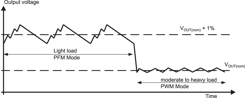 Figure 17. PFM Voltage Positioning
Pulling the MODE pin to DC ground results in an automatic transition between PFM and PWM modes to maximize efficiency.
The DC-DC converter output automatically discharges to ground through an internal 450-Ω load when EN_DCDC goes low or when the UVLO condition is met.
7.3.2 Soft Start
The step-down converter has an internal soft-start circuit that limits the inrush current during start-up. During soft start, the output voltage ramp-up is controlled as shown in Figure 18.
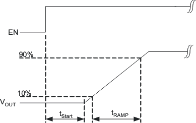 Figure 18. Soft Start
7.3.3 Linear Regulators
The two linear dropout regulators (LDOs) in the TPS65000-Q1 are designed to provide flexibility in system design. Each LDO has a separate voltage input and enable signal. The input can be tied to the output of the step-down converter or the output of another voltage source. Each LDO output discharges to ground automatically when EN_LDOx goes low.
A resistor network is needed to set the output voltage of the LDOs. Fixed-voltage output versions are also available; contact a TI sales representative for more information.
The LDOs are general-purpose devices that can handle inputs from 6 V down to 1.6 V. Figure 19 shows the necessary connections for LDO1. The same architecture applies to LDO2.
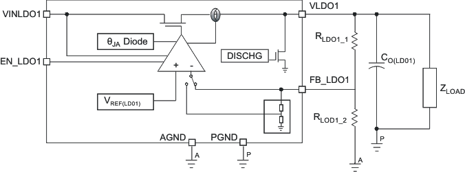 Figure 19. LDO Block Diagram and Output Voltage Setting
The output voltages of the LDOs are set by Equation 2:
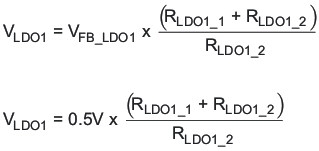
The combined resistance of RLDO1_1 and RLDO1_2 should be less than 1 MΩ.
7.3.4 Oscillator and Spread-Spectrum Clock Generation
The TPS65000-Q1 contains an internal oscillator running at a typical frequency of 2.25 MHz. This frequency is the fundamental switching frequency of the step-down converter when it is running in PWM mode. An additional circuit in the oscillator block implements spread-spectrum clocking, which modulates the main switching frequency when the device is in PWM mode. This spread-spectrum oscillation reduces the power that may cause EMI. When viewed in the frequency domain, the SSC spreads out the frequency that may introduce interference while simultaneously reducing the power. Because the frequency is continually shifting, the amount of time the switcher spends at any single frequency is reduced. This reduction in time means that the receiver that may see the interference has less time to integrate the interference.
Different spin versions of SSC settings are also possible; contact a TI sales representative for more information.
Figure 20 and Figure 21 show the advantage of SSC with the frequency spectrum centering on the nominal frequency 2.25 MHz. The blue spectrum is the result of the spread change. As shown in the figures, the harmonic spectrum is attenuated to 10 dB, compared to the same device without SSC.
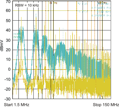 Figure 20. SSC On and Off Comparison from 1.5 MHz to 150 MHz
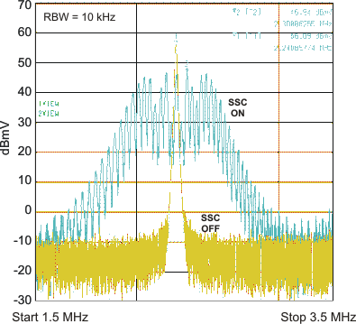 Figure 21. Zoom In of SSC On and Off Comparison from 1.5 MHz to 3.5 MHz
7.3.5 Power Good
The open-drain PG output is used to indicate the condition of the step-down converter and each LDO. This is a combined output, with the outputs being compared when the appropriate enable signal is high. The pin is pulled low when all enabled outputs are greater than 90% of the target voltage, and it is pulled into Hi-Z when an enabled output is less than 90% of its intended value or when all the enable signals are pulled low.
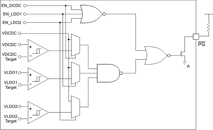 Figure 22. Power-Good Functionality
7.4 Device Functional Modes
The step-down converter has two modes of operation to maximize efficiency:
- PFM
- For light loads
- For automatic transition to between this mode and PWM mode automatically when MODE pin is pulled low over all load ranges
- To increase in output voltage setting by 1%
- For better accuracy
- PWM
