SLVS653C June 2008 – February 2016 TPS63010 , TPS63011 , TPS63012
PRODUCTION DATA.
- 1 Features
- 2 Applications
- 3 Description
- 4 Revision History
- 5 Device Comparison Table
- 6 Pin Configuration and Functions
- 7 Specifications
- 8 Detailed Description
- 9 Application and Implementation
- 10Power Supply Recommendations
- 11Layout
- 12Device and Documentation Support
- 13Mechanical, Packaging, and Orderable Information
9 Application and Implementation
NOTE
Information in the following applications sections is not part of the TI component specification, and TI does not warrant its accuracy or completeness. TI’s customers are responsible for determining suitability of components for their purposes. Customers should validate and test their design implementation to confirm system functionality.
9.1 Application Information
The TPS6301x are high-efficiency, low-quiescent current buck-boost converters suitable for application where the input voltage is higher, lower or equal to the output. Output currents can go as high as 1 A in boost mode and as high as 2 A in buck mode. The maximum average current in the switches is limited to a typical value of 2 A.
9.2 Typical Application
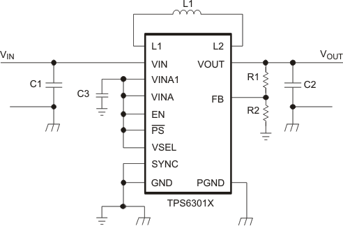 Figure 24. Adjustable Version
9.2.1 Design Requirements
The design guideline provides a component selection to operate the device within the recommended operating conditions. Table 2 lists the components for the Application Curves section.
Table 2. Components for Application Characteristic Curves
| REFERENCE | DESCRIPTION | MANUFACTURER |
|---|---|---|
| TPS6301 0 / 1 / 2 | Texas Instruments | |
| L1 | LPS3015-222 | Coilcraft |
| C1 | GRM188R60J106M (10 μF 6.3 V, 0603) | Murata |
| C2 | 2 × GRM188R60J106M (10 μF 6.3 V, 0603) | Murata |
| C3 | 0.1 μF, X7R ceramic | |
| R1, R2 | Depending on the output voltage at TPS63010, not used at TPS6301 1 / 2 (R1 shorted) |
9.2.2 Detailed Design Procedure
The TPS6301x DC-DC converters are intended for systems powered by one-cell Li-Ion or Li-Polymer battery with a typical voltage from 2.3 V to 4.5 V. They can also be used in systems powered by a double-cell or triple-cell Alkaline, NiCd, or NiMH battery with a typical terminal voltage from 2 V to 5.5 V. Additionally, any other voltage source with a typical output voltage from 2 V to 5.5 V can power systems where the TPS6301x is used.
9.2.2.1 Programming the Output Voltage
Within the TPS6301x family, there are fixed and adjustable output voltage versions available. To properly configure the fixed output voltage devices, the FB pin is used to sense the output voltage. This means that it must be connected directly to VOUT . At the adjustable output voltage versions, an external resistor divider is used to adjust the output voltage. The resistor divider must be connected between VOUT, FB, and GND. When the output voltage is regulated properly, the typical value of the voltage at the FB pin is 500 mV. The maximum recommended value for the output voltage is 5.5 V. The current through the resistive divider should be about 100 times greater than the current into the FB pin. The typical current into the FB pin is 0.01 μA, and the voltage across the resistor between FB and GND, R2, is typically 500 mV. Based on those two values, the recommended value for R2 should be lower than 500 kΩ, in order to set the divider current at 1 μA or higher. The recommended value for this resistor is in the range of 200 kΩ. From that, the value of the resistor connected between VOUT and FB. R1, depending on the needed output voltage (VOUT ), is calculated using Equation 1:

As an example, if an output voltage of 3.3 V is needed, a 1-MΩ resistor should be chosen for R1 if R2 is 180-kΩ.
 Figure 25. Typical Application Circuit for Adjustable Output Voltage Option
9.2.2.2 Inductor Selection
To properly configure the TPS6301x devices, an inductor must be connected between pin L1 and pin L2. To estimate the inductance value Equation 2 and Equation 3 can be used.


In Equation 2, the minimum inductance value L1 for step down mode operation is calculated. VIN1 is the maximum input voltage. In Equation 3 the minimum inductance, L2 , for boost mode operation is calculated. The recommended minimum inductor value is either L1 or L2 whichever is higher. As an example, a suitable inductor for generating 3.3 V from a Li-Ion battery with a battery voltage range from 2.5 V up to 4.2 V is 2.2 μH. The recommended inductor value range is between 1 μH and 4.7 μH. In general, this means that at high voltage conversion rates, higher inductor values offer better performance.
With the chosen inductance value, the peak current for the inductor in steady-state operation can be calculated. Equation 4 shows how to calculate the peak current I1 in step-down mode operation and Equation 5 shows how to calculate the peak current I2 in boost mode operation. VIN2 is the minimum input voltage.


The critical current value for selecting the right inductor is the higher value of I1 and I2. Consider that load transients and error conditions may cause higher inductor currents, especially when selecting an appropriate inductor. The following inductor series from different suppliers have been used with TPS6301x converters:
Table 3. List of Recommended Inductors
| VENDOR | INDUCTOR SERIES |
|---|---|
| Coilcraft | LPS3015 |
| LPS4012 | |
| FDK | MIPSA2520 |
| Murata | LQH3NP |
| LQM2HP | |
| Toko | FDSE0312 |
9.2.2.3 Capacitor Selection
9.2.2.3.1 Input Capacitor
At least a 4.7-μF input capacitor is recommended to improve transient behavior of the regulator and EMI behavior of the total power supply circuit. A ceramic capacitor placed as close as possible to the VIN and PGND pins of the IC is recommended.
9.2.2.3.2 Output Capacitor
For the output capacitor, TI recommends using small ceramic capacitors placed as close as possible to the VOUT and PGND pins of the IC. If, for any reason, the application requires the use of large capacitors which can not be placed close to the IC, using a smaller ceramic capacitor in parallel to the large one is recommended. This small capacitor should be placed as close as possible to the VOUT and PGND pins of the IC.
To get an estimate of the recommended minimum output capacitance, Equation 6 can be used.

A capacitor with a value in the range of the calculated minimum should be used. This is required to maintain control loop stability. There are no additional requirements regarding minimum ESR. There is also no upper limit for the output capacitance value. Larger capacitors will cause lower output voltage ripple as well as lower output voltage drop during load transients.
9.2.3 Application Curves
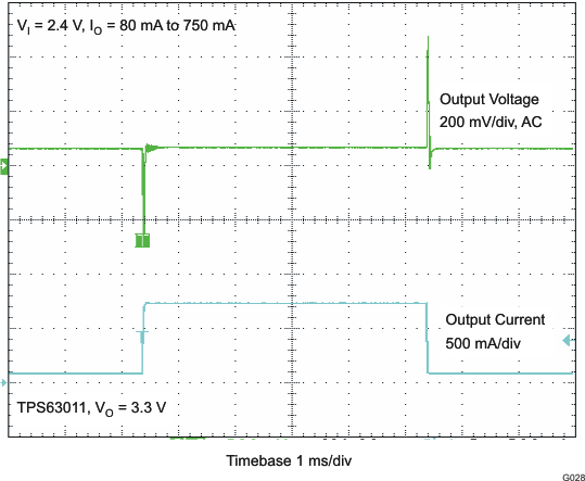 Figure 26. Load Transient Response (TPS63011)
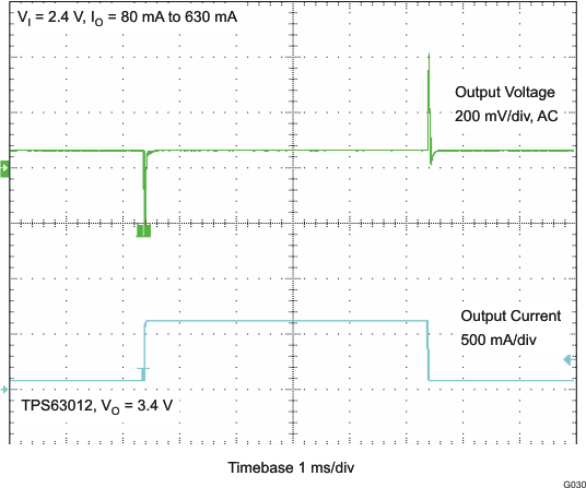 Figure 28. Load Transient Response (TPS63012)
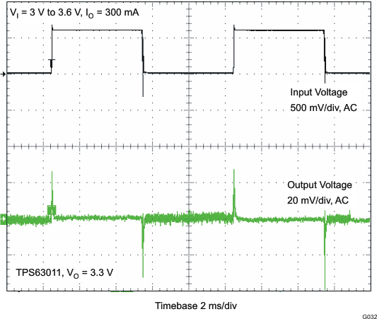 Figure 30. Line Transient Response (TPS63011)
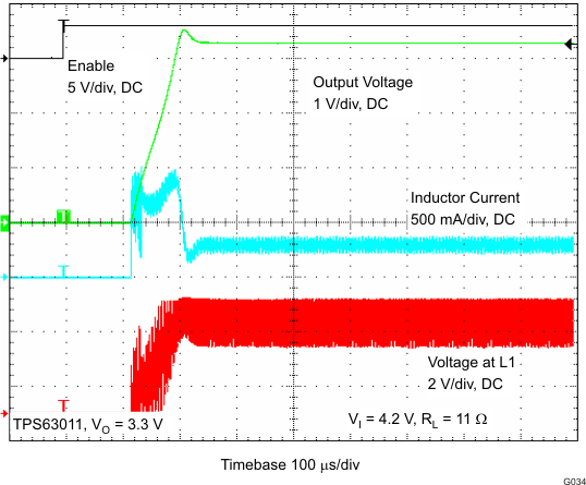 Figure 32. Start-Up After Enable (TPS63011)
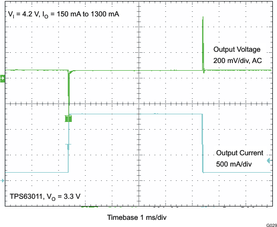 Figure 27. Load Transient Response (TPS63011)
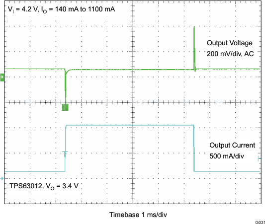 Figure 29. Load Transient Response (TPS63012)
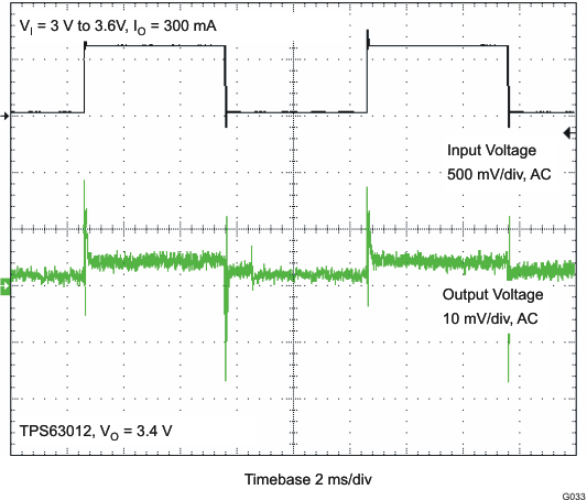 Figure 31. Line Transient Response (TPS63012)
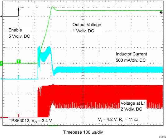 Figure 33. Start-Up After Enable (TPS63012)