ZHCS342B November   2013  – July 2014 TPS62740 , TPS62742

PRODUCTION DATA.  

  1. 特性
  2. 应用范围
  3. 说明
  4. 典型应用
  5. 修订历史记录
  6. Device Comparison Table
  7. Pin Configuration and Functions
  8. Specifications
    1. 8.1 Absolute Maximum Ratings
    2. 8.2 Handling Ratings
    3. 8.3 Recommended Operating Conditions
    4. 8.4 Thermal Information
    5. 8.5 Electrical Characteristics
    6. 8.6 Typical Characteristics
  9. Detailed Description
    1. 9.1 Overview
    2. 9.2 Functional Block Diagram
    3. 9.3 Feature Description
      1. 9.3.1 DCS-Control™
      2. 9.3.2 CTRL / Output Load
      3. 9.3.3 Enable / Shutdown
      4. 9.3.4 Power Good Output (PG)
      5. 9.3.5 Output Voltage Selection (VSEL1 - 4)
      6. 9.3.6 Softstart
      7. 9.3.7 Undervoltage Lockout UVLO
    4. 9.4 Device Functional Modes
      1. 9.4.1 VOUT And LOAD Output Discharge
      2. 9.4.2 Automatic Transition Into 100% Mode
      3. 9.4.3 Internal Current Limit
      4. 9.4.4 Dynamic Voltage Scaling with VSEL Interface
  10. 10Application and Implementation
    1. 10.1 Application Information
    2. 10.2 Typical Application
      1. 10.2.1 Design Requirements
      2. 10.2.2 Detailed Design Procedure
        1. 10.2.2.1 Inductor Selection
        2. 10.2.2.2 DC/DC Output Capacitor Selection
        3. 10.2.2.3 Input Capacitor Selection
      3. 10.2.3 Application Curves
    3. 10.3 System Example
  11. 11Power Supply Recommendations
  12. 12Layout
    1. 12.1 Layout Guidelines
    2. 12.2 Layout Example
  13. 13器件和文档支持
    1. 13.1 器件支持
      1. 13.1.1 第三方产品免责声明
    2. 13.2 文档支持
      1. 13.2.1 相关文档 
    3. 13.3 相关链接
    4. 13.4 商标
    5. 13.5 静电放电警告
    6. 13.6 术语表
  14. 14机械封装和可订购信息

封装选项

机械数据 (封装 | 引脚)
散热焊盘机械数据 (封装 | 引脚)
订购信息

12 Layout

12.1 Layout Guidelines

As for all switching power supplies, the layout is an important step in the design. Care must be taken in board layout to get the specified performance. If the layout is not carefully done, the regulator could show poor line and/or load regulation, stability issues as well as EMI problems and interference with RF circuits. It is critical to provide a low inductance, impedance ground path. Therefore, use wide and short traces for the main current paths. The input capacitor should be placed as close as possible to the IC pins VIN and GND. The output capacitor should be placed close between VOUT and GND pins. The VOUT line should be connected to the output capacitor and routed away from noisy components and traces (e.g. SW line) or other noise sources. The exposed thermal pad of the package and the GND pin should be connected. See Figure 53 for the recommended PCB layout.

12.2 Layout Example
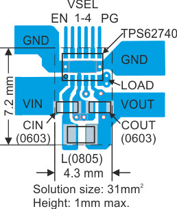
TPS62740 TPS62742 TPS62740_Layout_min.gifFigure 53. Recommended PCB Layout