SLVSBO4C October 2012 – December 2014 TPS62736 , TPS62737
UNLESS OTHERWISE NOTED, this document contains PRODUCTION DATA.
- 1 Features
- 2 Applications
- 3 Description
- 4 Revision History
- 5 Description (continued)
- 6 Device Voltage Options
- 7 Pin Configuration and Functions
- 8 Specifications
- 9 Detailed Description
- 10Application and Implementation
- 11Power Supply Recommendations
- 12Layout
- 13Device and Documentation Support
- 14Mechanical, Packaging, and Orderable Information
10 Application and Implementation
NOTE
Information in the following applications sections is not part of the TI component specification, and TI does not warrant its accuracy or completeness. TI’s customers are responsible for determining suitability of components for their purposes. Customers should validate and test their design implementation to confirm system functionality.
10.1 Application Information
The TPS62736/7 are step down DC-DC converters. Their low quiescent currents make them ideal for battery powered systems that are operated at low duty cycles in order to achieve low total power levels.
10.2 Typical Applications
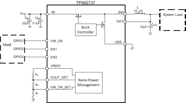
10.2.1 TPS62737 3-Resistor Typical Application Circuit
10.2.1.1 Design Requirements
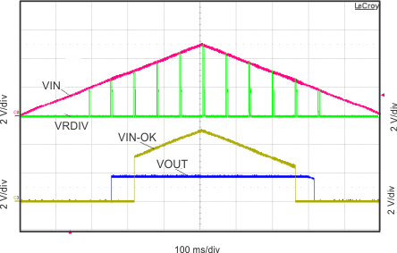
A 1.8-V, up to 200 mA regulated power rail is needed. The VIN_OK comparator should indicate when the input voltage drops below 2.9 V. No large load transients are expected.
10.2.1.2 Detailed Design Procedure
The recommended 10-µH inductor (TOKO DFE252012C) and 22-µF input capacitor are used. Since no large load transients are expected, the minimum 22-µF output capacitor is used. Had a large load transient been expected, we would have sized the capacitor using ITRAN = COUT x ΔVOUT / ΔTIME where ΔVOUT is amount of VOUT droop allowed for the time of the transient.
First set RSUM = R1 + R2 + R3 = 13 MΩ then solve Equation 2 for R1 = VBIAS x RSUM / VIN_OK = 1.21 V x 13 MΩ / 2.9 V = 5.42 MΩ → 5.49 MΩ as the closest 1 % resistor.
Then solve Equation 2 for R2 = VBIAS x RSUM / VOUT - R1 = 1.21 V x 13 MΩ / 1.8 V - 5.42 MΩ = 3.32 MΩ → 3.4 MΩ as the closest 1% resistor.
Finally R3 = RSUM - R1 - R2 = 13 MΩ - 5.42 MΩ - 3.32 MΩ = 4.26 MΩ → 4.32 MΩ as the closest 1% resistor.
These values yield VOUT = 1.79 V and VIN_OK threshold = 2.91 V.
If using 4 resistors, see Resistor Selection for guidance on sizing the resistors.
10.2.1.2.1 Inductor Selection
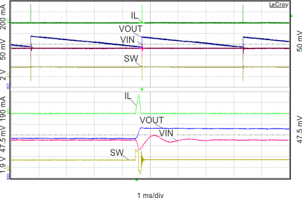
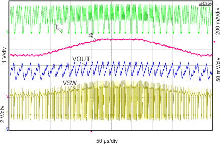
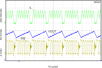
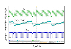
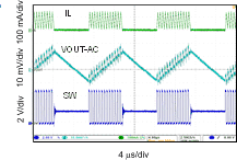
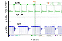
The internal-control circuitry is designed to control the switching behavior with a nominal inductance of 10 µH ± 20%. The saturation current of the inductor' should be at least 25% higher than the maximum cycle-by-cycle current limit per the electrical specs table (ILIM) in order to account for load transients. Because this device is a hysteretic controller, it is a naturally stable system (single order transfer function). However, the smaller the inductor value is, the faster the switching currents are. The speed of the peak current detect circuit sets the inductor of the TPS62736 lower bound to 4.7 µH. When using a 4.7 µH, the peak inductor current will increase when compared to that of a 10-µH inductor. The steady-state operation with a 4.7-µH inductor with a 50-mA load for the TPS62736 is shown in Figure 65.
A list of inductors recommended for this device is shown in Table 4.
Table 4. Recommended Inductors
| INDUCTANCE (µH) | DIMENSIONS (mm) | PART NUMBER | MANUFACTURER |
|---|---|---|---|
| 10 | 2.0 x 2.5 x 1.2 | DFE252012C-H-100M | Toko |
| 10 | 4.0 x 4.0 x 1.7 | LPS4018-103M | Coilcraft |
| 4.7 (TPS62736 only) | 2.0 x 2.5 x 1.2 | DFE252012R-H-4R7M | Toko |
10.2.1.2.2 Output Capacitor Selection
The output capacitor is chosen based on transient response behavior and ripple magnitude. The lower the capacitor value, the larger the ripple will become and the larger the droop will be in the case of a transient response. It is recommended to use at least a 22-µF output capacitor for most applications.
10.2.1.2.3 Input Capacitor Selection
The bulk input capacitance is recommended to be a minimum of 4.7 µF ± 20% for the TPS62736 and 22 µF ± 20% for the TPS62737. This bulk capacitance is used to suppress the lower frequency transients produced by the switching converter. There is no upper bound to the input-bulk capacitance. In addition, a high-frequency bypass capacitor of 0.1 µF is recommended in parallel with the bulk capacitor. The high-frequency bypass is used to suppress the high-frequency transients produced by the switching converter.
10.2.1.2.4 Resistor Selection
Equation 1 to Equation 4 are the equations for sizing the external resistors to set the VIN_OK threshold and VOUT regulation value. The spreadsheet at SLVC489 can help size the external resistors.
10.2.1.3 Application Curves
See efficiency, line regulation, and load regulation curves at Figure 30, Figure 37, and Figure 36.
| V(IN) = 3.6 V bench power supply | ||
| R(OUT) = 100 kΩ |
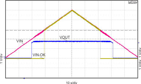
| V(IN) = power amplifier ramped from 0 V to 5 V to 0 V | ||
| V(IN) = 3.6 V -> 4.6 V -> 4.6 V from bench power supply | ||
| R(OUT) = 9 Ω | ||
| V(IN) = power amplifier ramped from 0 V to 5 V to 0 V | ||
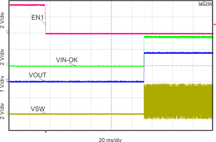
| EN1 = low; EN2 = high | ||
VIN
| V(IN) = 3.6 V bench power supply | ||
| EN1 = low; EN2 transitioned from low to high | ||
| R(OUT) = 1 kΩ |
| V(IN) = 3.6 V bench power supply | ||
| R(OUT) = 9 Ω |
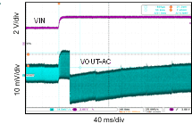
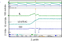
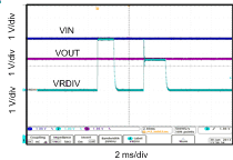
| V(IN) = 3.6 V bench power supply + additional C(IN) = 100 uF | ||
| R(OUT) = open to 9 Ω to open | ||
| V(IN) = 4.0 V bench supply + additional C(IN) = 100 uF | ||
| VOUT resistors modified to provide 2.5 V | ||
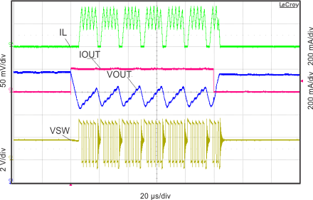
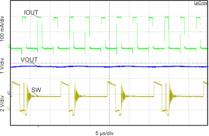
| I(OUT) = 200 mA every 1 us |
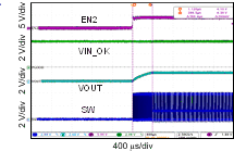
| V(IN) = 3.6 V bench power supply | ||
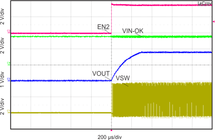
| EN2 = high; EN1 transitioned from high to low | ||
| R(OUT) = 1 kΩ |
10.2.2 TPS62736 4-Resistor Typical Application Circuit
 Figure 62. TPS62736 4-Resistor Typical Application Circuit
10.2.2.1 Design Requirements
A 2.5-V, up to 50-mA regulated power rail is needed. The VIN_OK comparator should indicate when the input voltage drops below 2.9 V. No large load transients are expected.
10.2.2.2 Detailed Design Procedure
The recommended 10-µH inductor (TOKO DFE252012C) and 4.7-µF input capacitor are used. Since no large load transients are expected, the minimum 22-µF output capacitor is used. Had a large load transient been expected, we would have sized the capacitor using ITRAN = COUT x ΔVOUT / ΔTIME where ΔVOUT is amount of VOUT droop allowed for the time of the transient.
First set RSUM = R1 + R2 = R3 + R4 = 13 MΩ then solve Equation 4 for R1 = VBIAS x RSUM / VIN_OK = 1.21 V x 13 MΩ / 2.9 V = 5.42 MΩ → 5.36 MΩ as the closest 1 % resistor.
Then R2 = RSUM - R1 = 13 MΩ - 5.42 MΩ = 7.58 MΩ → 7.5 MΩ as the closest 1% resistor.
Solve Equation 3 for R4 = VBIAS x RSUM / VOUT = 1.21 V x 13 MΩ / 2.5 V = 6.29 MΩ → 6.34 MΩ as the closest 1% resistor.
Finally R3 = RSUM - R3 = 13 MΩ - 6.29 MΩ = 6.71 MΩ → 6.81 MΩ as the closest 1% resistor.
These values yield VOUT = 2.51 V and VIN_OK threshold = 2.90 V.
If using 3 resistors, see Resistor Selection for guidance on sizing the resistors.
10.2.2.3 Application Curves
See efficiency, load regulation and line regulation graphs at Figure 1, Figure 7 and Figure 8 respectively.
| V(IN) = 3.0 V bench power supply | ||
| R(OUT) = 50 Ω |
| V(IN) = 3.0 V bench power supply | ||
| VOUT resistors changed to provide 1.8 V; L = 4.7 uH | ||
| R(OUT) = 100 kΩ |
| V(IN) = 3.0 V -> 5.0 V from bench power supply | ||
| R(OUT) = 50 Ω | ||
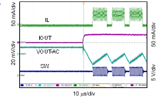
| V(IN) = 4.0 V from bench power supply + additional CIN = 100 uF | ||
| I(OUT) = 200 mA every 1us | ||
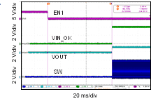
| V(IN) = 4.0 V from bench power supply | ||
| VOUT resistors modified to provide 1.8 V | ||
| EN1 = low, EN2 transitioned low to high |
| V(IN) = 3.0 V bench power supply | ||
| R(OUT) = 100 kΩ |
| V(IN) = 3.0 V bench power supply | ||
| V(IN) = 4.0 V from bench power supply + additional CIN = 100 uF | ||
| R(OUT) = open - > 50 Ω |
| V(IN) = 4.0 V from bench power supply | ||
| VOUT resistors modified to provide 1.8 V | ||
| EN2 = high, EN1 transitioned high to low | ||