ZHCS174C January 2014 – October 2014 TPS61230 , TPS61232
UNLESS OTHERWISE NOTED, this document contains PRODUCTION DATA.
- 1 特性
- 2 应用范围
- 3 说明
- 4 修订历史记录
- 5 Device Comparison Table
- 6 Pin Configuration and Functions
- 7 Specifications
- 8 Detailed Description
-
9 Applications and Implementation
- 9.1 Application Information
- 9.2
Typical Applications
- 9.2.1 TPS61230 2.3-V to 5.5-V Input, 5-V Output Converter
- 9.2.2 TPS61230 2.3-V to 5.5-V Input, 3.5-V Output Converter
- 9.2.3 TPS61230 Application with Feed Forward Capacitor for Best Transient Response
- 10Power Supply Recommendations
- 11Layout
- 12器件和文档支持
- 13机械封装和可订购信息
11 Layout
11.1 Layout Guidelines
For all switching power supplies, the layout is an important step in the design, especially at high peak currents and high switching frequencies. If the layout is not carefully done, the regulator could show stability problems as well as EMI problems. Therefore, use wide and short traces for the main current path and for the power ground tracks. The input capacitor, output capacitor, and the inductor should be placed as close as possible to the IC. Use a common ground node for power ground and a different one for control ground to minimize the effects of ground noise. Connect these ground nodes at the GND pin of the IC. The most critical current path for all boost converters is from the switching FET, through the synchronous FET, then the output capacitors, and back to ground of the switching FET. Therefore, the output capacitors and their traces should be placed on the same board layer as the IC and as close as possible between the IC’s VOUT and GND pin.
See Figure 37 for the recommended layout.
11.2 Layout Example
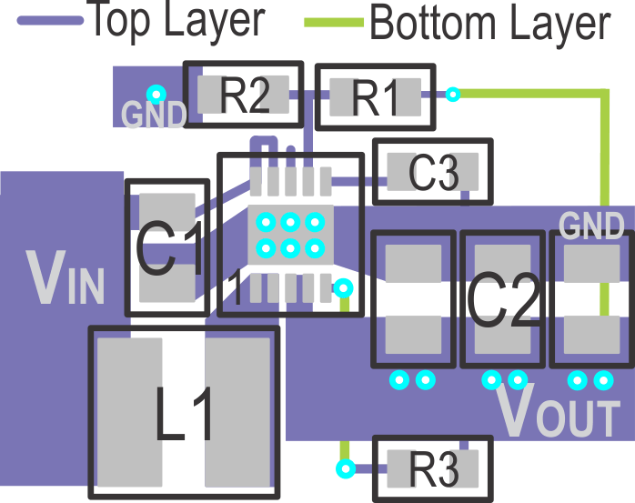 Figure 37. Layout Recommendation
11.3 Thermal Considerations
Implementation of integrated circuits in low-profile and fine-pitch surface-mount packages typically requires special attention to power dissipation. Many system-dependent issues such as thermal coupling, airflow, added heat sinks and convection surfaces, and the presence of other heat-generating components affect the power-dissipation limits of a given component.
Two basic approaches for enhancing thermal performance are listed below.
- Improving the power dissipation capability of the PCB design
- Introducing airflow in the system
For more details on how to use the thermal parameters in the dissipation ratings table please check the application report Thermal Characteristics of Linear and Logic Packages Using JEDEC PCB Designs (SZZA017) and the application report Semiconductor and IC Package Thermal Metrics (SPRA953).