SLVSBG1D October 2012 – May 2015 TPS61196
PRODUCTION DATA.
- 1 Features
- 2 Applications
- 3 Description
- 4 Revision History
- 5 Pin Configuration and Functions
- 6 Specifications
-
7 Detailed Description
- 7.1 Overview
- 7.2 Functional Block Diagram
- 7.3 Feature Description
- 7.4
Device Functional Modes
- 7.4.1
Protections
- 7.4.1.1 Switch Current Limit Protection Using the ISNS Pin
- 7.4.1.2 LED Open Protection
- 7.4.1.3 LED Short-Cross Protection Using the FBP Pin
- 7.4.1.4 Schottky Diode Open Protection
- 7.4.1.5 Schottky Diode Short Protection
- 7.4.1.6 IFB Overvoltage Protection During Start-up
- 7.4.1.7 Output Overvoltage Protection Using the OVP Pin
- 7.4.1.8 Output Short-to-Ground Protection
- 7.4.1.9 IFB Short-to-Ground Protection
- 7.4.1.10 ISET Short-to-Ground Protection
- 7.4.1.11 Thermal Protection
- 7.4.2 Indication For Fault Conditions
- 7.4.1
Protections
- 8 Application and Implementation
- 9 Power Supply Recommendations
- 10Layout
- 11Device and Documentation Support
- 12Mechanical, Packaging, and Orderable Information
封装选项
机械数据 (封装 | 引脚)
- PWP|28
散热焊盘机械数据 (封装 | 引脚)
- PWP|28
订购信息
1 Features
- 8-V to 30-V Input Voltage
- Up to 120-V Output Voltage
- 100-KHz to 800-kHz Programmable Switching Frequency
- Adaptive Boost Output for LED Voltages
- Six Current Sinks, 200-mA Continuous Output, 400-mA Pulse Output for Each String
- ±1.5% Current Matching Between Strings
- High Precision PWM Dimming Resolution up to 5000:1
- Programmable Overvoltage Threshold at Output and Each Current Sink
- Programmable Undervoltage Threshold at Input with Adjustable Hysteresis
- Adjustable Soft Start Time Independent of Dimming Duty Cycle
- Built-in LED Open and LED Short Protection
- Built-in Schottky Diode Open/Short Protection
- Built-in ISET Short Protection
- Built-in IFB Short Protection
- Thermal Shutdown
2 Applications
- LCD TV Backlight
- Scan Mode LCD TV Backlight
3 Description
The TPS61196 provides a highly integrated solution for LCD TV backlight with an independent PWM dimming function for each string. This device is a current mode boost controller driving up to six WLED strings with multiple LEDs in series. Each string has an independent current regulator providing a LED current adjustable from 50 mA to 400 mA within ±1.5% matching accuracy. The minimal voltage at the current sink is programmable in the range of 0.3 V to 1 V to fit with different LED current settings. The input voltage range for the device is from 8 V to 30 V.
The device adjusts the boost controller's output voltage automatically to provide only the voltage required by the LED string with the largest forward voltage drop plus the minimum required voltage at that string's IFB pin, thereby optimizing driver efficiency. Its switching frequency is programmed by an external resistor from 100 kHz to 800 kHz.
The TPS61196 supports direct PWM brightness dimming. Each string has an independent PWM control input. During the PWM dimming, the LED current is turned on or turned off at the frequency and duty cycle which are determined by the external PWM signal. The PWM frequency ranges from 90 Hz to 22 kHz.
The device integrates overcurrent protection, output short-circuit protection, ISET short-to-ground protection, diode open and short protection, LED open and short protection, and overtemperature shutdown circuit. In addition, the TPS61196 can detect the IFB pin short to ground to protect the LED string. The device also provides programmable input undervoltage lockout threshold and output overvoltage protection threshold.
The TPS61196 has a built-in linear regulator which steps down the input voltage to the VDD voltage for powering the internal circuitry. An soft-start circuit is implemented internally to work with an external capacitor to adjust the soft start-up time to minimize the in-rush current during boost converter start-up. The device is available in a 28-pin HTSSOP package with PowerPAD™.
Device Information(1)
| PART NUMBER | PACKAGE | BODY SIZE (NOM) |
|---|---|---|
| TPS61196 | HTSSOP (28) | 9.70 mm x 4.40 mm |
- For all available packages, see the orderable addendum at the end of the datasheet.
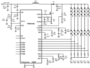
Simplified Schematic

4 Revision History
Changes from C Revision (March 2013) to D Revision
- Added Device Information and ESD Rating tables, Feature Description, Device Functional Modes, Application and Implementation, Power Supply Recommendations, Layout, Device and Documentation Support, and Mechanical, Packaging, and Orderable Information sections; moved some curves to Application Curves section; remove Device Comparison tableGo
- Changed location of several specs from EC table to Switching CharGo
Changes from B Revision (January 2013) to C Revision
- Changed VL max value from 1.0 V to 0.8 VGo
- Changed VIN = 7 V to VIN = 8 V in Test Conditions for VISNS(OC)Go
Changes from A Revision (November 2012) to B Revision
- Changed RPD max value from 2.4 MΩ to 3.0 MΩGo
- Changed VISET min value from 1.220 V to 1.217 VGo
- Deleted IFLT_L max valueGo
- Changed R7 to R9 in Table 1Go
Changes from * Revision (October 2012) to A Revision