ZHCSD24 October 2014 TPS61169
PRODUCTION DATA.
- 1 特性
- 2 应用
- 3 说明
- 4 简化电路原理图
- 5 修订历史记录
- 6 Pin Configuration and Functions
- 7 Specifications
- 8 Detailed Description
- 9 Application and Implementation
- 10Power Supply Recommendations
- 11Layout
- 12器件和文档支持
- 13机械封装和可订购信息
11 Layout
11.1 Layout Guidelines
As for all switching power supplies, especially those high frequency and high current ones, layout is an important design step. If layout is not carefully done, the regulator could suffer from instability as well as noise problems. Therefore, use wide and short traces for high current paths. The input capacitor CIN needs to be close to VIN pin and GND pin in order to reduce the input ripple seen by the IC. If possible choose higher capacitance value for it. The SW pin carries high current with fast rising and falling edge, therefore, the connection between the SW pin to the inductor should be kept as short and wide as possible. The output capacitor COUT should be put close to VOUT pin. It is also beneficial to have the ground of COUT close to the GND pin since there is large ground return current flowing between them. FB resistor should be put close to FB pin. When laying out signal ground, it is recommended to use short traces separated from power ground traces, and connect them together at a single point close to the GND pin.
11.2 Layout Example
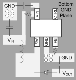 Figure 18. TPS61169 Board Layout