SLVS538B NOVEMBER 2004 – December 2014 TPS61060 , TPS61061 , TPS61062
PRODUCTION DATA.
- 1 Features
- 2 Applications
- 3 Description
- 4 Revision History
- 5 Device Comparison Table
- 6 Pin Configuration and Functions
- 7 Specifications
- 8 Detailed Description
- 9 Application and Implementation
- 10Power Supply Recommendations
- 11Layout
- 12Device and Documentation Support
- 13Mechanical, Packaging, and Orderable Information
封装选项
请参考 PDF 数据表获取器件具体的封装图。
机械数据 (封装 | 引脚)
- YZF|8
- DRB|8
散热焊盘机械数据 (封装 | 引脚)
- DRB|8
订购信息
6 Pin Configuration and Functions
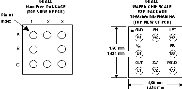
8-Pin 3x3-mm QFN Package
Top View
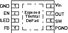
Pin Functions
| PIN | I/O | DESCRIPTION | ||
|---|---|---|---|---|
| NAME | NO. | |||
| CSP | QFN | |||
| VIN | B1 | 8 | I | Input supply pin of the device |
| EN | A2 | 2 | I | Enable pin. This pin needs to be pulled high to enable the device. To allow brightness control of the LEDs, a PWM signal up to 1 kHz can be applied. This pin has an internal pulldown resistor. |
| GND | A1 | 1 | Analog ground | |
| PGND | C3 | 5 | Power ground | |
| FB | B3 | 4 | I | This is the feedback pin of the device. The feedback pin regulates the LED current through the sense resistor by regulating the voltage across Rs. The feedback voltage is set by the ILED pin. ILED=GND sets the feedback voltage to 500 mV. ILED=high sets the feedback voltage to 250 mV. Refer to digital brightness control section for more information. |
| OUT | C1 | 7 | O | Output of the device |
| SW | C2 | 6 | I | Switch pin of the device |
| ILED | A3 | 3 | I | Digital brightness control input. When this pin is grounded, the digital brightness control is disabled. When this pin is connected to high, then the feedback voltage is reduced to typically 250 mV and the digital brightness control is enabled. Refer to digital brightness control section for more information. |
| PowerPAD™ | – | – | The PowerPAD™ (exposed thermal diepad) is only available on the QFN package. The PowerPAD™ needs to be connected and soldered to analog ground (GND). | |