SLVS391C October 2001 – September 2015 TPS60500 , TPS60501 , TPS60502 , TPS60503
PRODUCTION DATA.
- 1 Features
- 2 Applications
- 3 Description
- 4 Revision History
- 5 Device Comparison Table
- 6 Pin Configuration and Functions
- 7 Specifications
- 8 Detailed Description
- 9 Application and Implementation
- 10Power Supply Recommendations
- 11Layout
- 12Device and Documentation Support
- 13Mechanical, Packaging, and Orderable Information
9 Application and Implementation
NOTE
Information in the following applications sections is not part of the TI component specification, and TI does not warrant its accuracy or completeness. TI’s customers are responsible for determining suitability of components for their purposes. Customers should validate and test their design implementation to confirm system functionality.
9.1 Application Information
The TPS6050x devices are switched capacitor voltage converters providing fractional conversion to achieve high efficiency over a wide input and output voltage range. They support regulated output voltages of 3.3 V, 1.8 V and 1.5 V or adjustable output voltages from a 1.8-V to 6.5-V input voltage range.
9.2 Typical Applications
9.2.1 Typical Application Circuit for Fixed-Voltage and Adjustable-Voltage Versions
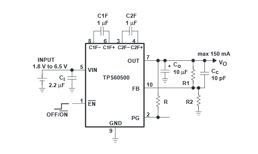 Figure 7. Typical Operating Circuit – TPS60500, Adjustable Output Voltage
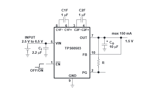 Figure 8. Typical Operating Circuit – TPS60503, Maximum 150-mA Output Current
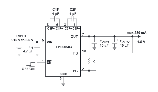 Figure 9. Typical Operating Circuit – TPS60503, Maximum 250-mA Output Current
9.2.1.1 Design Requirements
The Detailed Design Procedure provides a component selection to operate the device within the recommended operating conditions
Figure 7, Figure 8 and Figure 9 show the typical operation circuits. The TPS60501 to TPS60503 devices use an internal resistor divider for sensing the output voltage. The FB pin must be connected externally with the output. For maximum output current and best performance, four ceramic capacitors are recommended. For lower currents or higher allowed output voltage ripple, other capacitors can also be used. TI recommends that the minimum value of the output capacitor be 4.7 µF. This value is necessary to maintain a stable operation of the system. Flying capacitors lower than 1 µF can be used, but this decreases the maximum output power. This means that the device works in linear mode with lower output currents. The device works in the linear mode for an output current of greater than 150 mA. With an output current greater than 150 mA, an output capacitor of ≥22 µF must be used. Figure 9 shows that two 10-µF capacitors can also be used in parallel.
9.2.1.2 Detailed Design Procedure
9.2.1.2.1 Capacitor Selection
Designed specifically for space-critical battery-powered applications, the complete converter requires only four external capacitors. The capacitor values are closely linked to the required output current, output noise, and ripple requirements. The input capacitor improves system efficiency by reducing the input impedance, and it also stabilizes the input current. The value of the output capacitor, CO, influences the stability of the voltage regulator. The minimum required capacitance for CO is 4.7 µF. Depending on the maximum allowed output ripple voltage and load current, larger values can be chosen. For an output current greater than 150 mA, a minimum output capacitor of 22 µF is required. Table 2 shows ceramic capacitor values recommended for low output voltage ripple.
Table 1. Recommended Capacitor Values
| IOUT, MAX
[mA] |
CIN
[µF] |
C(xF)
[µF] |
COUT
[µF] |
|---|---|---|---|
| 50 | 2.2 | 0.22 | 4.7 |
| 150 | 4.7 | 1 | 10 |
| 250 | 4.7 | 1 | 22 |
Table 2. Recommended Capacitors
| MANUFACTURER | PART NUMBER | SIZE | CAPACITANCE | TYPE |
|---|---|---|---|---|
| Taiyo Yuden | LMK212BJ105KG LMK212BJ225MG EMK316BJ225KL LMK316BJ475KL JMK316BJ106KL |
805 805 1206 1206 1206 |
1 µF 2.2 µF 2.2 µF 4.7 µF 10 µF |
Ceramic Ceramic Ceramic Ceramic Ceramic |
| TDK | C2012X5R1C105M C2012X5R1A225M C2012X5R0J106M |
805 805 805 |
1 µF 2.2 µF 10 µF/6.3 V |
Ceramic Ceramic Ceramic |
Table 3 contains a list of manufacturers of ceramic capacitors. Ceramic capacitors provide the lowest output voltage ripple because they typically have the lowest ESR-rating.
Table 3. Recommended Capacitor Manufacturers
| MANUFACTURER | CAPACITOR TYPE | INTERNET |
|---|---|---|
| Taiyo Yuden | X7R/X5R ceramic | www.t−yuden.com |
| TDK | X7R/X5R ceramic | www.component.tdk.com |
| Vishay | X7R/X5R ceramic | www.vishay.com |
| Kemet | X7R/X5R ceramic | www.kemet.com |
9.2.1.2.2 Resistor Combinations
Table 4. Resistor Combinations
| NOMINAL OUTPUT VOLTAGE | EQUATION | POSSIBLE E24 RESISTOR COMBINATIONS |
|---|---|---|
| 1.2 V | R1 = 0.5R2 | R1 = 100 kΩ, R2 = 200 kΩ, (1.20 V) |
| 1.5 V | R1 = 0.875R2 | R1 = 160 kΩ, R2 = 180 kΩ, (1.51 V) |
| 1.6 V | R1 = R2 | any |
| 1.8 V | R1 = 1.25R2 | R1 = 150 kΩ, R2 = 120 kΩ, (1.80 V) |
| 2.5 V | R1 = 2.125R2 | R1 = 510 kΩ, R2 = 240 kΩ, (2.50 V) |
| R1 = 470 kΩ, R2 = 220 kΩ, (2.51 V) |
Equations:


9.2.1.3 Application Curves
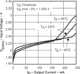
Minimum Input Voltage vs Output Current
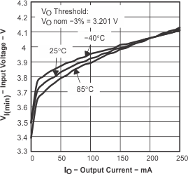
Minimum Input Voltage vs Output Current
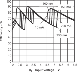
Efficiency vs Input Voltage
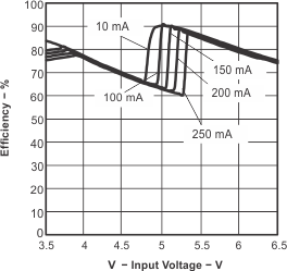
Efficiency vs Input Voltage
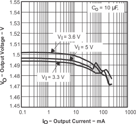
Output Voltage vs Output Current
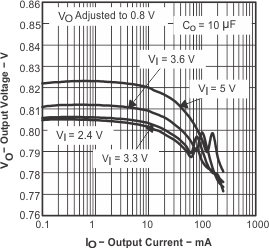
Output Voltage vs Output Current
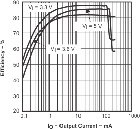
Efficiency vs Output Current
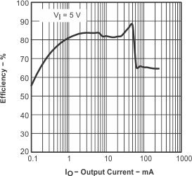
Efficiency vs Output Current
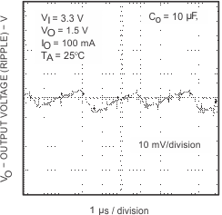
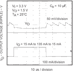
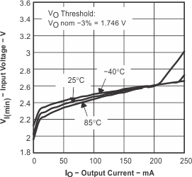
Minimum Input Voltage vs Output Current
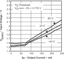
Minimum Input Voltage vs Output Current
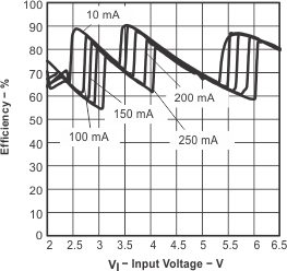
Efficiency vs Input Voltage
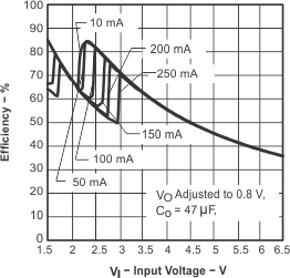
Efficiency vs Input Voltage
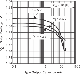
Output Voltage vs Output Current
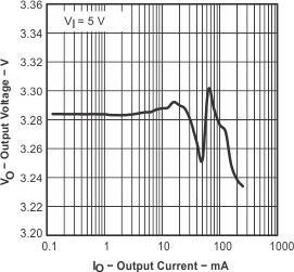
Output Voltage vs Output Current
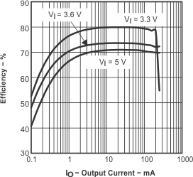
Efficiency vs Output Current
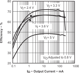
Efficiency vs Output Current
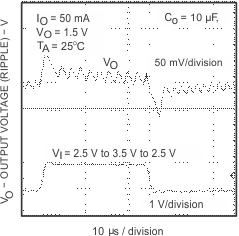
9.3 System Examples
9.3.1 DSP Supply With Sequencing
This application shows a power supply for a typical digital signal processor (DSP). DSPs usually have core voltages in the 1-V to 2.5-V range, whereas the voltage at the I/O-pins (I/O voltage) is typically 3.3 V to interface with external logic and converters. Therefore, a power supply with two output voltages is required. The application works with an input voltage in the range of 3.5 V to 6.5 V. The maximum output current is 150 mA on each output.
The supply is enabled by pulling the enable pin (EN of the TPS60503) to GND. The step-down charge pump starts and its power good (PG) output goes high. This enables the LDO which powers the I/O lines and generates a reset signal for the DSP. Figure 29 shows the timing diagram of the start-up or shutdown procedure.
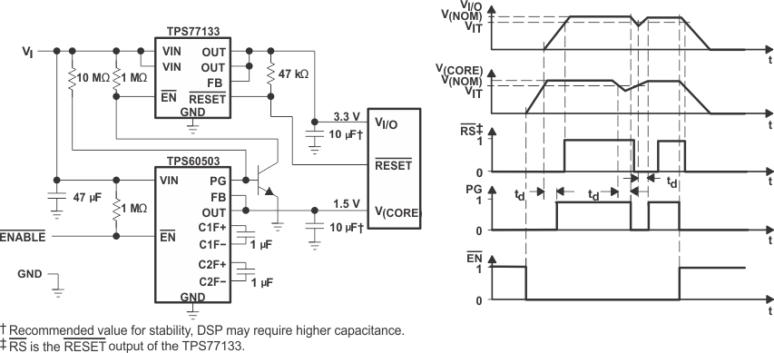 Figure 29. DSP Supply With Sequencing
9.3.2 LC-Post Filter
If the output voltage ripple of the step-down charge pump is to high, an LC post filter can be used.
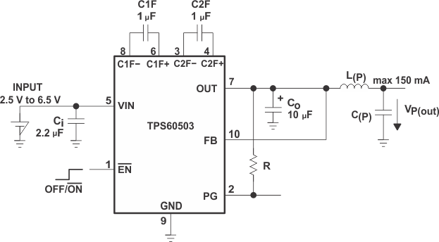 Figure 30. LC-Post Filter
Table 5. Measurement Results on Different C(fly), C(P), L(P) Combinations; BW = 500 MHz
| VI
[V] |
IO
[mA] |
CI
[µF] |
C(XF)
[µF] |
CO
[µF] |
L(P)
[µH] |
C(P)
[µF] |
VO
[V] |
TYPICAL VP(Out) VPP[mV] | TYPICAL VO(RMS) [mV] |
|---|---|---|---|---|---|---|---|---|---|
| CERAMIC | CERAMIC | CERAMIC | CERAMIC | ||||||
| 5 | 50 | 2.2 | 0.22 | 4.7 | — | 0.1 (X7R) | 3.3 | 50 | 8 |
| 5 | 50 | 2.2 | 0.22 | 4.7 | — | 0.1 (X7R) | 1.5 | 30 | 9 |
| 5 | 150 | 4.7 | 1 | 10 | — | 0.1 (X7R) | 1.5 | 50 | 6 |
| 5 | 250 | 4.7 | 1 | 2 x 10 | — | 0.1 (X7R) | 1.5 | 45 | 8 |
| 5 | 100 | 4.7 | 1 | 10 | 0.1 | 0.1 (X7R) | 1.5 | 20 | 4 |
9.3.3 Power Supply With Dynamic Voltage Scaling
Dynamic voltage scaling of the core can be used to reduce power consumption of a digital signal processor (DSP). During the periods, in which the maximum DSP performance is not required, the core voltage can be reduced when the DSP operates at a lower clock-rate. This function is called runtime power control (RPC) and is supported by modern DSPs. RPC extends battery lifetime in handheld applications, like MP3 players and digital cameras.
The supply of DSPs is separated into I/O interface and core supply. Interface is mostly powered by a 3.3-V system supply, whereas core supply achieves voltages far below 1.5 V. The TPS60500 is powered by the 3.3-V system supply. The DSP itself selects the applied core voltage.
The core voltage is switched between 1.5 V and 1.1 V by changing the feedback resistor network. A MOSFET modifies the voltage divider at the feedback (FB) pin by switching a resistor. In this application, a general-purpose MOSFET BSS138 is used with a VGS(th) of 1.6 V. A DSP 3.3-V I/O port drives the gate. The feedback resistor network consists of R2, R3 and R4. C(ff) is the fast-forward capacitor for improved line regulation.
General requirements for the application:
- Output voltage1 (DSP core): 1.5 V ±0.08 V
- Output voltage 2 (DSP core): 1.1 V +0.1 V –0.05 V
- Input voltage: 3 V to 3.3 V
- Output current: 150 mA (10R load)
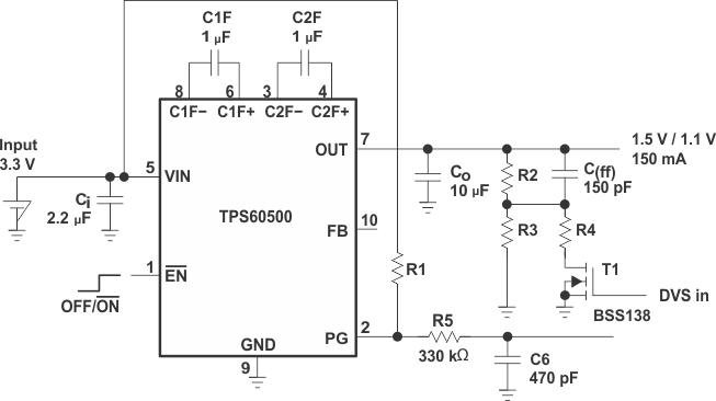 Figure 31. Dynamic Voltage Scaling Application
To keep current through the adjustment resistor network as low as possible, the resistors are calculated to:


9.3.4 Internet Audio Power Supply
The input voltage from a single or dual NiCd, NiMH or alkaline cell is boosted to 3.3 V. This voltage is used as system supply for the application and as an input voltage for the step-down charge pump which is used to provide the core voltage for a DSP.
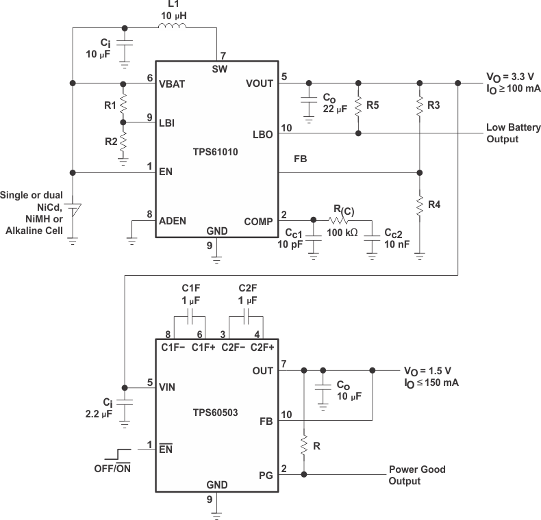 Figure 32. Internet Audio Power Supply