SLVS391C October   2001  – September 2015 TPS60500 , TPS60501 , TPS60502 , TPS60503

PRODUCTION DATA.  

  1. Features
  2. Applications
  3. Description
  4. Revision History
  5. Device Comparison Table
  6. Pin Configuration and Functions
  7. Specifications
    1. 7.1 Absolute Maximum Ratings
    2. 7.2 ESD Ratings
    3. 7.3 Recommended Operating Conditions
    4. 7.4 Thermal Information
    5. 7.5 Electrical Characteristics
    6. 7.6 Typical Characteristics
  8. Detailed Description
    1. 8.1 Overview
    2. 8.2 Functional Block Diagram
    3. 8.3 Feature Description
      1. 8.3.1 Short-Circuit Current Limit and Thermal Protection
      2. 8.3.2 Enable
      3. 8.3.3 Power Good Detector
    4. 8.4 Device Functional Modes
      1. 8.4.1 Start-up Procedure
      2. 8.4.2 Conversion Modes
        1. 8.4.2.1 LDO Conversion Mode
        2. 8.4.2.2 2/3x Conversion Mode
        3. 8.4.2.3 0.5x Conversion Mode
        4. 8.4.2.4 1/3x Conversion Mode
  9. Application and Implementation
    1. 9.1 Application Information
    2. 9.2 Typical Applications
      1. 9.2.1 Typical Application Circuit for Fixed-Voltage and Adjustable-Voltage Versions
        1. 9.2.1.1 Design Requirements
        2. 9.2.1.2 Detailed Design Procedure
          1. 9.2.1.2.1 Capacitor Selection
          2. 9.2.1.2.2 Resistor Combinations
        3. 9.2.1.3 Application Curves
    3. 9.3 System Examples
      1. 9.3.1 DSP Supply With Sequencing
      2. 9.3.2 LC-Post Filter
      3. 9.3.3 Power Supply With Dynamic Voltage Scaling
      4. 9.3.4 Internet Audio Power Supply
  10. 10Power Supply Recommendations
  11. 11Layout
    1. 11.1 Layout Guidelines
    2. 11.2 Layout Examples
  12. 12Device and Documentation Support
    1. 12.1 Device Support
      1. 12.1.1 Third-Party Products Disclaimer
    2. 12.2 Related Links
    3. 12.3 Community Resources
    4. 12.4 Trademarks
    5. 12.5 Electrostatic Discharge Caution
    6. 12.6 Glossary
  13. 13Mechanical, Packaging, and Orderable Information

封装选项

机械数据 (封装 | 引脚)
散热焊盘机械数据 (封装 | 引脚)
订购信息

11 Layout

11.1 Layout Guidelines

All capacitors must be soldered as close as possible to the IC. A PCB layout proposal for a two-layer board is shown in Figure 33. Connect all capacitors as close as possible to the circuit to achieve optimized output voltage ripple performance.

11.2 Layout Examples
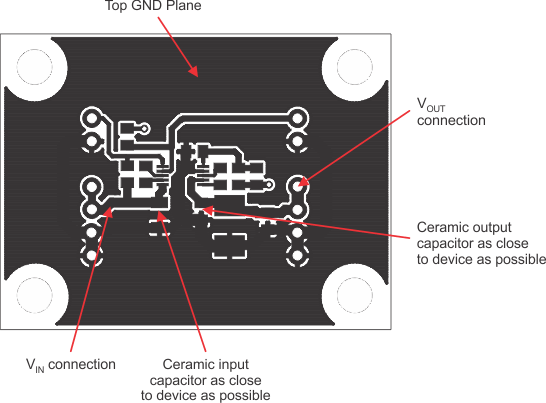
TPS60500 TPS60501 TPS60502 TPS60503 layoutexample1_b.gif Figure 33. Recommended PCB Layout for TPS6050x (Top Layer)
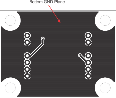
TPS60500 TPS60501 TPS60502 TPS60503 layoutexample2.gif Figure 34. Recommended PCB Layout for TPS6050x (Bottom Layer)
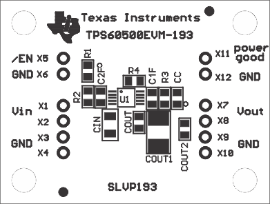
TPS60500 TPS60501 TPS60502 TPS60503 layoutexample1_a.gif Figure 35. Top Silkscreen