SLVS274A March 2000 – April 2016 TPS60200 , TPS60201 , TPS60202 , TPS60203
PRODUCTION DATA.
- 1 Features
- 2 Applications
- 3 Description
- 4 Revision History
- 5 Device Comparison Tables
- 6 Pin Configuration and Functions
- 7 Specifications
- 8 Detailed Description
- 9 Application and Implementation
- 10Power Supply Recommendations
- 11Layout
- 12Device and Documentation Support
- 13Mechanical, Packaging, and Orderable Information
8 Detailed Description
8.1 Overview
The TPS6020x charge pumps provide a regulated 3.3-V output from a 1.8-V to 3.6-V input. They deliver up to 100-mA load current while maintaining the output at 3.3 V ± 4%. Designed specifically for space-critical, battery-powered applications, the complete converter requires only four external capacitors. The device is using the push-pull topology to achieve lowest output voltage ripple. The converter is also optimized for smallest board space. It makes use of small-sized capacitors, with the highest output current rating per output capacitance and package size.
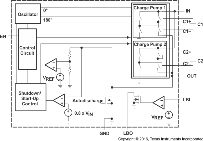
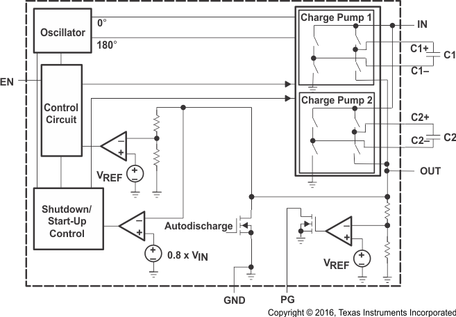
The TPS6020x circuits consist of an oscillator, a 1.18-V voltage reference, an internal resistive feedback circuit, an error amplifier, two charge pump power stages with high current MOSFET switches, a shutdown and start-up circuit, a control circuit, and an auto-discharge transistor (see Functional Block Diagrams).
8.2 Functional Block Diagrams
 Figure 2. TPS60200 and TPS60202 With Low-Battery Detector
 Figure 3. TPS60201 and TPS60203 With Power-Good Detector
8.3 Feature Description
8.3.1 Start-Up, Shutdown, and Auto-Discharge
During start-up, that is when EN is set from logic low to logic high, the output capacitor is directly connected to IN and charged up with a limited current until the output voltage VO reaches 0.8 × VI. When the start-up comparator detects this limit, the converter begins switching. This precharging of the output capacitor guarantees a short start-up time. In addition, the inrush current into an empty output capacitor is limited. The converter can start into a full load, which is defined by a 33-Ω or 66-Ω resistor, respectively.
Driving EN low disables the converter. This disables all internal circuits and reduces the supply current to only 0.05 μA. The device exits shutdown once EN is set high. When the device is disabled, the load is isolated from the input. This is an important feature in battery-operated products because it extends the products shelf life.
Additionally, the output capacitor will automatically be discharged after EN is taken low. This ensures that the system, when switched off, is in a stable and reliable condition because the supply voltage is removed from the supply pins.
8.3.2 Synchronization to an External Clock Signal
The operating frequency of the charge pump is limited to 400 kHz to avoid interference in the sensitive 455-kHz IF band. The device can either run from the integrated oscillator, or an external clock signal can be used to drive the charge pump. The maximum frequency of the external clock signal is 800 kHz. The switching frequency used internally to drive the charge pump power stages is half of the external clock frequency. The external clock signal is applied to the EN pin. The device will switch off if the signal on EN is hold low for more than 10 μs.
When the load current drops below the LinSkip current threshold, the devices will enter the pulse-skip mode but stay synchronized to the external clock signal.
8.3.3 Power-Good Detector
The power-good output is an open-drain output that pulls low when the output is out of regulation. When the output rises to within 90% of its nominal voltage, the power-good output is released. Power-good is high impedance in shutdown. In normal operation, an external pullup resistor must be connected between PG and OUT, or any other voltage rail in the appropriate range. The resistor should be in the 100-kΩ to 1-MΩ range. If the PG output is not used, it should remain unconnected.
8.4 Device Functional Modes
8.4.1 Push-Pull Operating Mode
The two single-ended charge pump power stages operate in the so-called push-pull operating mode, that is they operate with a 180°C phase shift. Each single-ended charge pump transfers charge into its transfer capacitor (C1 or C2) in one half of the period. During the other half of the period (transfer phase), the transfer capacitor is placed in series with the input to transfer its charge to CO. While one single-ended charge pump is in the charge phase, the other one is in the transfer phase. This operation assures an almost constant output current which ensures a low output ripple.
If the clock were to run continuously, this process would eventually generate an output voltage equal to two times the input voltage (hence the name voltage doubler). To provide a regulated fixed output voltage of 3.3 V, the TPS6020x devices use either pulse-skip or constant-frequency linear-regulation control mode. The mode is automatically selected based on the output current. If the load current is below the LinSkip current threshold, it switches into the power-saving pulse-skip mode to boost efficiency at low output power.
8.4.2 Constant-Frequency Mode
When the output current is higher then the LinSkip current threshold, the charge pump runs continuously at the switching frequency f(OSC). The control circuit, fed from the error amplifier, controls the charge on C1 and C2 by controlling the gates and hence the rDS(ON) of the integrated MOSFETs. When the output voltage decreases, the gate drive increases, resulting in a larger voltage across C1 and C2. This regulation scheme minimizes output ripple. Since the device switches continuously, the output signal contains well-defined frequency components, and the circuit requires smaller external capacitors for a given output ripple. However, constant-frequency mode, due to higher operating current, is less efficient at light loads. For this reason, the device switches seamlessly into the pulse-skip mode when the output current drops below the LinSkip current threshold.
8.4.3 Pulse-Skip Mode
The regulator enters the pulse-skip mode when the output current is lower than the LinSkip current threshold of
7 mA. In the pulse-skip mode, the error amplifier disables switching of the power stages when it detects an output voltage higher than 3.3 V. The controller skips switching cycles until the output voltage drops below 3.3 V. Then the error amplifier reactivates the oscillator and switching of the power stages starts again. A 30-mV output voltage offset is introduced in this mode.
The pulse-skip regulation mode minimizes operating current because it does not switch continuously and deactivates all functions except the voltage reference and error amplifier when the output is higher than 3.3 V. Even in pulse-skip mode the rDS(ON) of the MOSFETs is controlled. This way the energy per switching cycle that is transferred by the charge pump from the input to the output is limited to the minimum that is necessary to sustain a regulated output voltage, with the benefit that the output ripple is kept to a minimum. When switching is disabled from the error amplifier, the load is also isolated from the input.