ZHCSJH9A August   2019  – August 2019 TPS56C230

PRODUCTION DATA.  

  1. 特性
  2. 应用
  3. 说明
    1.     Device Images
      1.      简化原理图
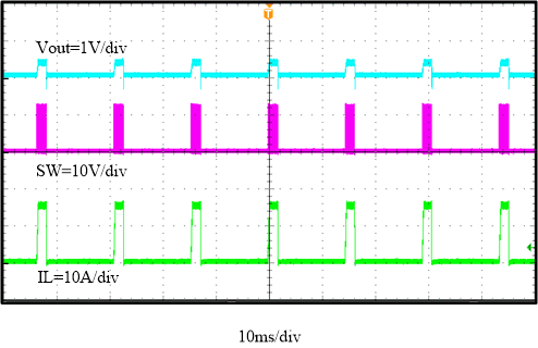
      2.      效率与输出电流 Eco-mode
  4. 修订历史记录
  5. Pin Configuration and Functions
    1.     Pin Functions
  6. Specifications
    1. 6.1 Absolute Maximum Ratings
    2. 6.2 ESD Ratings
    3. 6.3 Recommended Operating Conditions
    4. 6.4 Thermal Information
    5. 6.5 Electrical Characteristics
    6. 6.6 Typical Characteristics
  7. Detailed Description
    1. 7.1 Overview
    2. 7.2 Functional Block Diagram
    3. 7.3 Feature Description
      1. 7.3.1  PWM Operation and D-CAP3 Control
      2. 7.3.2  Soft Start
      3. 7.3.3  Large Duty Operation
      4. 7.3.4  Power Good
      5. 7.3.5  Overcurrent Protection and Undervoltage Protection
      6. 7.3.6  Overvoltage Protection
      7. 7.3.7  Out-of-Bounds Operation
      8. 7.3.8  UVLO Protection
      9. 7.3.9  Output Voltage Discharge
      10. 7.3.10 Thermal Shutdown
    4. 7.4 Device Functional Modes
      1. 7.4.1 Light Load Operation
      2. 7.4.2 Eco-mode Control
      3. 7.4.3 Force CCM
      4. 7.4.4 Mode Selection
      5. 7.4.5 Standby Operation
  8. Application and Implementation
    1. 8.1 Application Information
    2. 8.2 Typical Application
      1. 8.2.1 Design Requirements
      2. 8.2.2 Detailed Design Procedure
        1. 8.2.2.1 Custom Design With WEBENCH® Tools
        2. 8.2.2.2 Output Voltage Set Point
        3. 8.2.2.3 MODE Selection
        4. 8.2.2.4 Inductor Selection
        5. 8.2.2.5 Output Capacitor Selection
        6. 8.2.2.6 Input Capacitor Selection
      3. 8.2.3 Application Curves
  9. Power Supply Recommendations
  10. 10Layout
    1. 10.1 Layout Guidelines
    2. 10.2 Layout Example
  11. 11器件和文档支持
    1. 11.1 器件支持
      1. 11.1.1 第三方产品免责声明
      2. 11.1.2 开发支持
        1. 11.1.2.1 使用 WEBENCH® 工具创建定制设计
    2. 11.2 接收文档更新通知
    3. 11.3 社区资源
    4. 11.4 商标
    5. 11.5 静电放电警告
    6. 11.6 Glossary
  12. 12机械、封装和可订购信息

封装选项

机械数据 (封装 | 引脚)
散热焊盘机械数据 (封装 | 引脚)
订购信息

Application Curves

Figure 19 through Figure 34 apply to the circuit of Figure 18. VIN = 12 V. TA = 25°C unless otherwise specified.
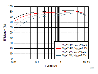
TPS56C230 D000-Efficiency1.gif
Figure 19. Efficiency Curve
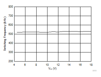
TPS56C230 D033-Fswline1.gif
IOUT = 12 A
Figure 21. Switching Frequency vs Input Voltage
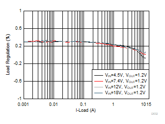
TPS56C230 D032-LoadRegulation.gif
Figure 20. Load Regulation
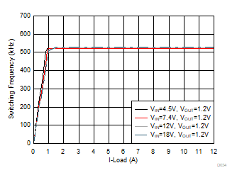
TPS56C230 D034-Fswload1.gif
Figure 22. Switching Frequency vs Output Load
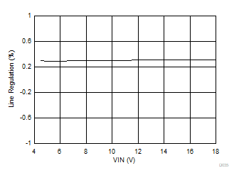
TPS56C230 D035-LineReg1.gif
IOUT=0.1A
Figure 23. Line Regulation
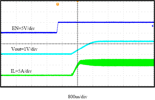
TPS56C230 fbd-03-slvsde4.gif
IOUT = 6A
Figure 25. Start-Up Through EN
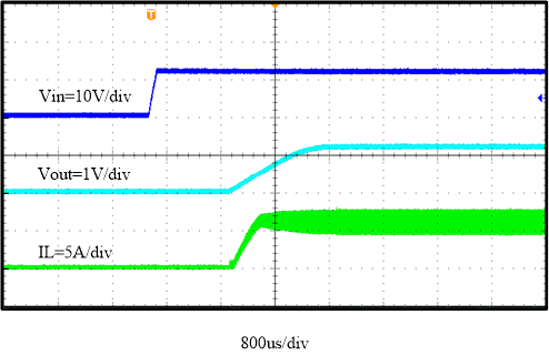
TPS56C230 fbd-01-slvsde4.gif
IOUT = 6 A
Figure 27. Start Up Relative to VIN Rising
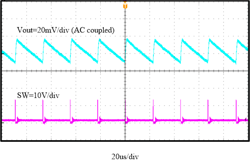
TPS56C230 fbd-05-slvsde4.gif
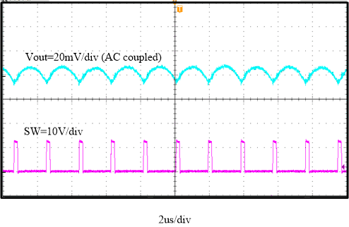
IOUT = 0.1 A
Figure 29. Output Voltage Ripple
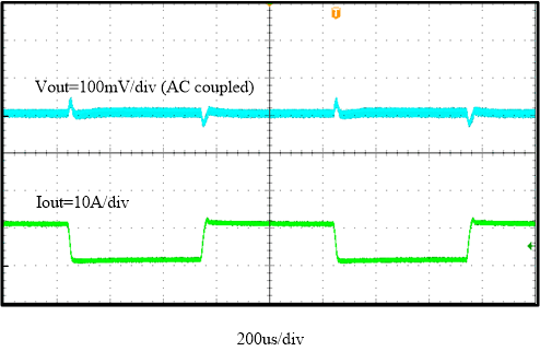
TPS56C230 fbd-07-slvsde4.gif
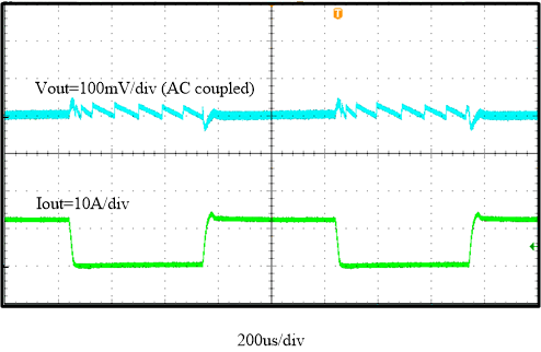
1.2 A to 10.8 A Slew Rate=2.5A/us
Figure 31. Transient Response
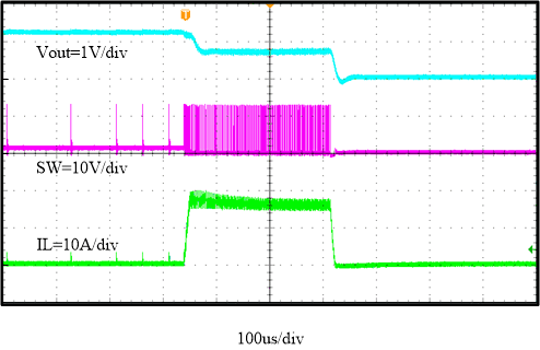
TPS56C230 fbd-09-slvsde4.gif
Figure 33. Normal Operation to Output Hard Short
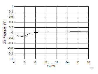
TPS56C230 D036-LineReg2.gif
IOUT=12A
Figure 24. Line Regulation
TPS56C230 fbd-04-slvsde4.gif
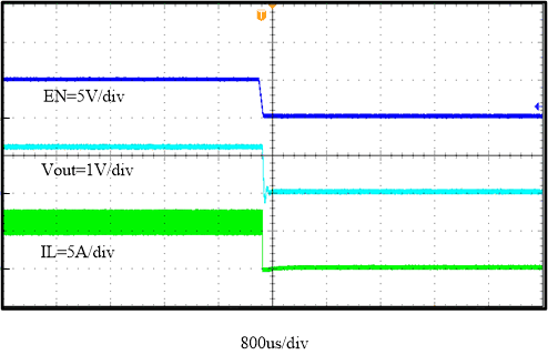
IOUT = 6A
Figure 26. Shut-down Through EN
TPS56C230 fbd-02-slvsde4.gif
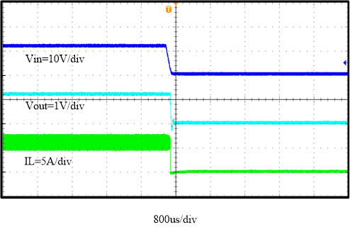
IOUT = 6 A
Figure 28. Shut Down Relative to VIN Falling
TPS56C230 fbd-06-slvsde4.gif
IOUT = 12 A
Figure 30. Output Voltage Ripple
TPS56C230 fbd-08-slvsde4.gif
0 A to 12 A Slew Rate=2.5A/us
Figure 32. Transient Response
TPS56C230 fbd-10-slvsde4.gif
Figure 34. Output Hard Short Hiccup Protection