ZHCSDI6A March   2015  – March 2015 TPS566250

PRODUCTION DATA.  

  1. 特性
  2. 应用
  3. 说明
  4. 简化电路原理图
  5. 修订历史记录
  6. Pin Configuration and Functions
  7. Specifications
    1. 7.1 Absolute Maximum Ratings
    2. 7.2 ESD Ratings
    3. 7.3 Recommended Operating Conditions
    4. 7.4 Thermal Information
    5. 7.5 Electrical Characteristics
    6. 7.6 Timing Requirements
    7. 7.7 Typical Characteristics
  8. Detailed Description
    1. 8.1 Overview
    2. 8.2 Functional Block Diagram
    3. 8.3 Feature Description
      1. 8.3.1 PWM Operation
      2. 8.3.2 PWM Frequency and Adaptive On-Time Control
      3. 8.3.3 Soft Start and Pre-Biased Soft Start
      4. 8.3.4 Overcurrent Protection
      5. 8.3.5 UVLO Protection
      6. 8.3.6 Thermal Shutdown
    4. 8.4 Device Functional Modes
      1. 8.4.1 Auto-Skip Eco-mode™ Control
    5. 8.5 Programming
      1. 8.5.1 I2C Interface
      2. 8.5.2 I2C Protocol
        1. 8.5.2.1 Input Voltage
        2. 8.5.2.2 Output Voltage
        3. 8.5.2.3 Data Format
        4. 8.5.2.4 START and STOP Conditions
      3. 8.5.3 I2C Chip Address Byte
    6. 8.6 Register Maps
      1. 8.6.1 I2C Register Address Byte
        1. 8.6.1.1 Output Voltage Register (offset = 00000000) [reset = 0h]
        2. 8.6.1.2 Power Good State Register (offset = 00011000) [reset = 18h]
      2. 8.6.2 CheckSum Bit
      3. 8.6.3 Output Voltage Registers
      4. 8.6.4 Summary of Default Control Bits
        1. 8.6.4.1 DAC Settle
        2. 8.6.4.2 Operation During VID Transition
  9. Applications and Implementation
    1. 9.1 Application Information
    2. 9.2 Typical Application
      1. 9.2.1 Design Requirements
      2. 9.2.2 Detailed Design Procedure
        1. 9.2.2.1 Output Voltage Resistors Selection
        2. 9.2.2.2 Output Filter Selection
        3. 9.2.2.3 Input Capacitor Selection
        4. 9.2.2.4 Bootstrap Capacitor Selection
      3. 9.2.3 Application Performance Curves
  10. 10Power Supply Recommendations
  11. 11Layout
    1. 11.1 Layout Guidelines
    2. 11.2 Layout Example
  12. 12器件和文档支持
    1. 12.1 文档支持
    2. 12.2 商标
    3. 12.3 静电放电警告
    4. 12.4 术语表
  13. 13机械封装和可订购信息
    1. 13.1 热性能信息

封装选项

机械数据 (封装 | 引脚)
散热焊盘机械数据 (封装 | 引脚)
订购信息

6 Pin Configuration and Functions

TPS566250
8-Pin DDA
(Top View)
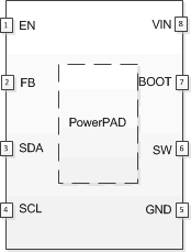
TPS566250 po_slvscv3.gif

Pin Functions

PIN I/O DESCRIPTION
NAME NO.
BOOT 7 I/O Supply input for high-side NFET gate drive circuit. Connect 0.1-µF ceramic capacitor between VBST and SW pins.
EN 1 I Enable input control. Pull High to enable converter.
FB 2 I Converter feedback input. Connect to output voltage with resistor divider.
GND 5 Power ground
SCL 4 I/O Clock I/O terminal.
SDA 3 I/O Data I/O terminal.
SW 6 I/O Switch node connections for both the high-side NFET and low–side NFET.
VIN 8 I Input voltage supply pin.
PowerPAD™ Thermal pad of the package. Must be soldered down to operate normally and achieve appropriate power dissipation. Connect sensitive FB returns to GND at a single point.