ZHCSI44A April   2018  – December 2018 TPS563249

PRODUCTION DATA.  

  1. 特性
  2. 应用
  3. 说明
    1.     Device Images
      1.      简化原理图
      2.      TPS563249 效率
  4. 修订历史记录
  5. Pin Configuration and Functions
    1.     Pin Functions
  6. Specifications
    1. 6.1 Absolute Maximum Ratings
    2. 6.2 ESD Ratings
    3. 6.3 Recommended Operating Conditions
    4. 6.4 Thermal Information
    5. 6.5 Electrical Characteristics
    6. 6.6 Typical Characteristics
  7. Detailed Description
    1. 7.1 Overview
    2. 7.2 Functional Block Diagram
    3. 7.3 Feature Description
      1. 7.3.1 Adaptive On-Time Control and PWM Operation
      2. 7.3.2 Soft Start and Pre-Biased Soft Start
      3. 7.3.3 Current Protection
      4. 7.3.4 Undervoltage Lockout (UVLO) Protection
      5. 7.3.5 Thermal Shutdown
    4. 7.4 Device Functional Modes
      1. 7.4.1 Normal Operation
      2. 7.4.2 Standby Operation
  8. Application and Implementation
    1. 8.1 Application Information
    2. 8.2 Typical Application
      1. 8.2.1 Design Requirements
      2. 8.2.2 Detailed Design Procedure
        1. 8.2.2.1 Output Voltage Resistors Selection
        2. 8.2.2.2 Output Filter Selection
        3. 8.2.2.3 Input Capacitor Selection
        4. 8.2.2.4 Bootstrap Capacitor Selection
        5. 8.2.2.5 Dropout
      3. 8.2.3 Application Curves
  9. Power Supply Recommendations
  10. 10Layout
    1. 10.1 Layout Guidelines
    2. 10.2 Layout Example
  11. 11器件和文档支持
    1. 11.1 接收文档更新通知
    2. 11.2 社区资源
    3. 11.3 商标
    4. 11.4 静电放电警告
    5. 11.5 术语表
  12. 12机械、封装和可订购信息

封装选项

机械数据 (封装 | 引脚)
散热焊盘机械数据 (封装 | 引脚)
订购信息

Application Curves

TA = 25°C, VIN = 12 V (unless otherwise noted)
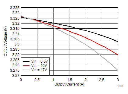
TPS563249 Load_reg_SLVSE54_2p0.gif
Figure 18. Load Regulation
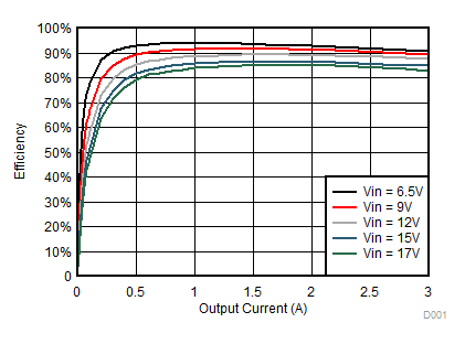
TPS563249 Eff of 3.3Vout_2p0.gif
Figure 20. Efficiency
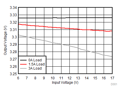
TPS563249 Line_reg_SLVSE54_2p0.gif
Figure 19. Line Regulation
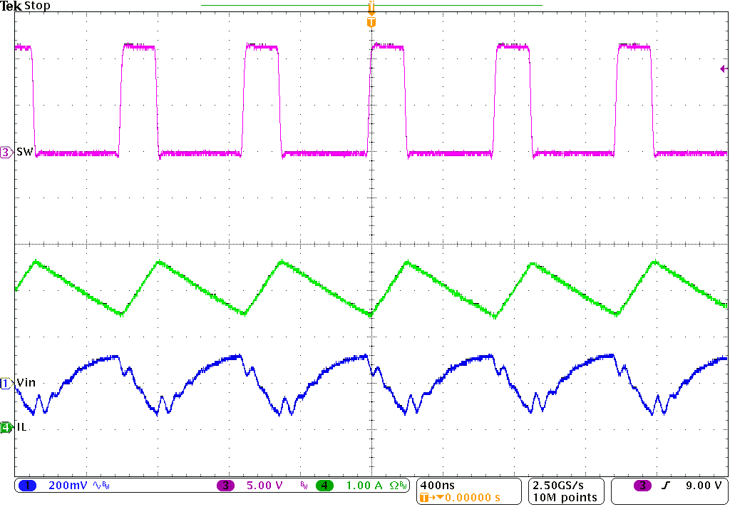
TPS563249 Vin ripple 3A_2p0.png
Iout = 3 A
Figure 21. Input Voltage Ripple
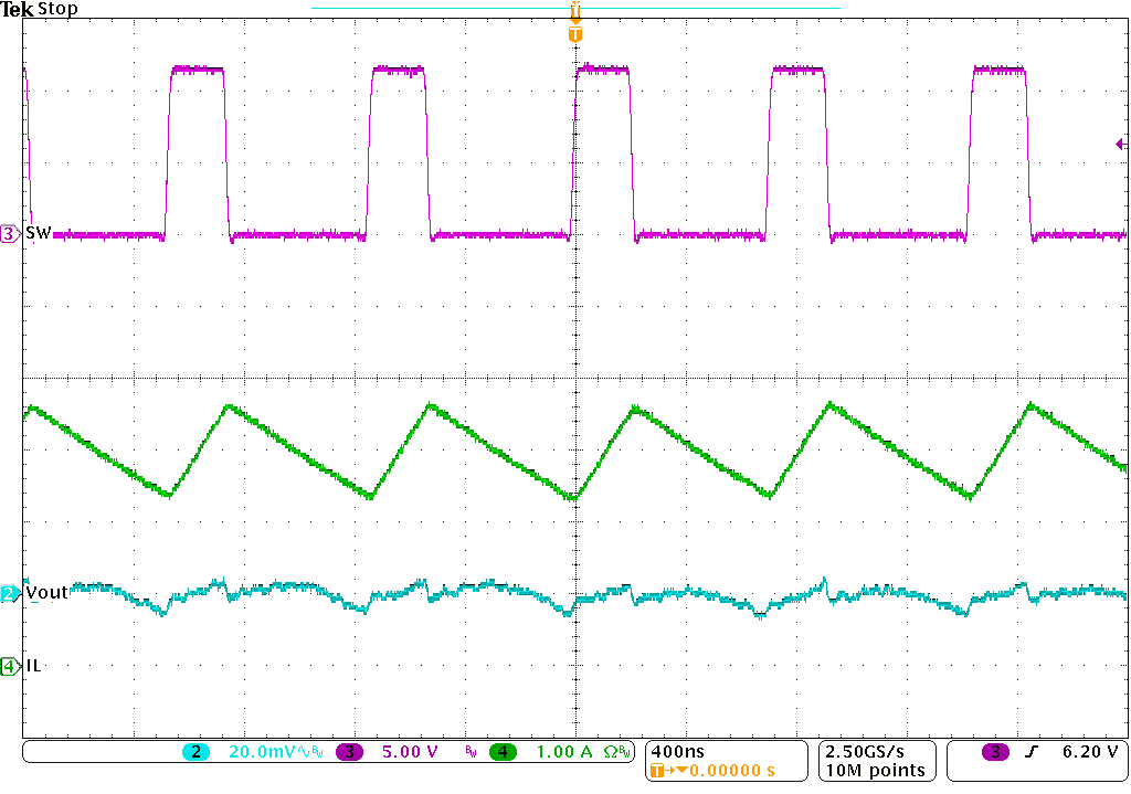
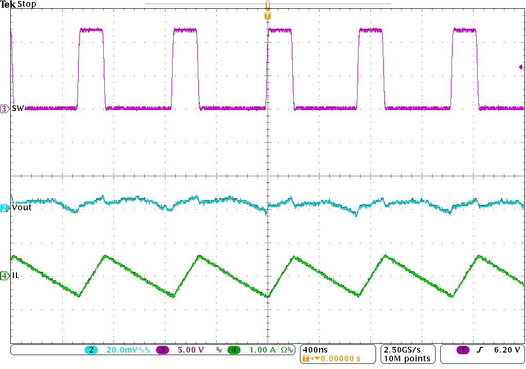
TPS563249 Vout ripple 3A_2p0.png
Iout = 3 A
Figure 22. Output Voltage Ripple
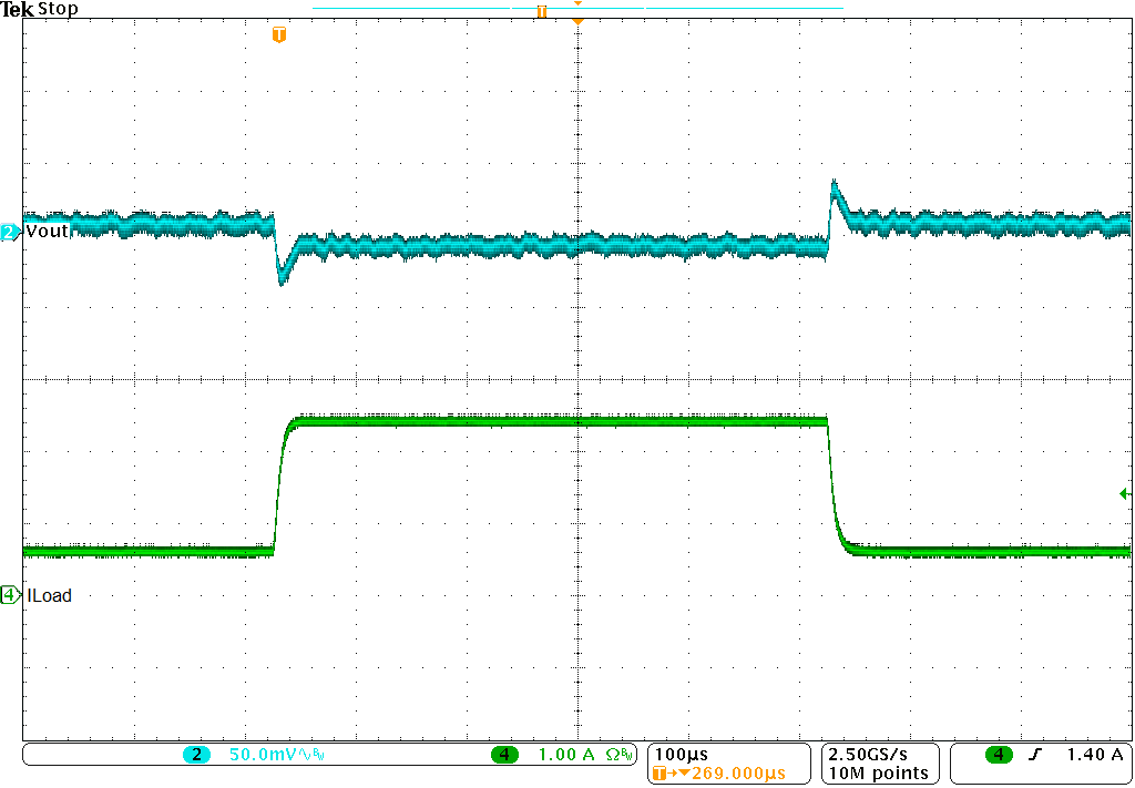
TPS563249 load tran 0.6to2.4A 1.6A-us_2p0.png
Slew rate is 1.6 A/µS
Figure 24. Transient Response, 0.6 to 2.4 A
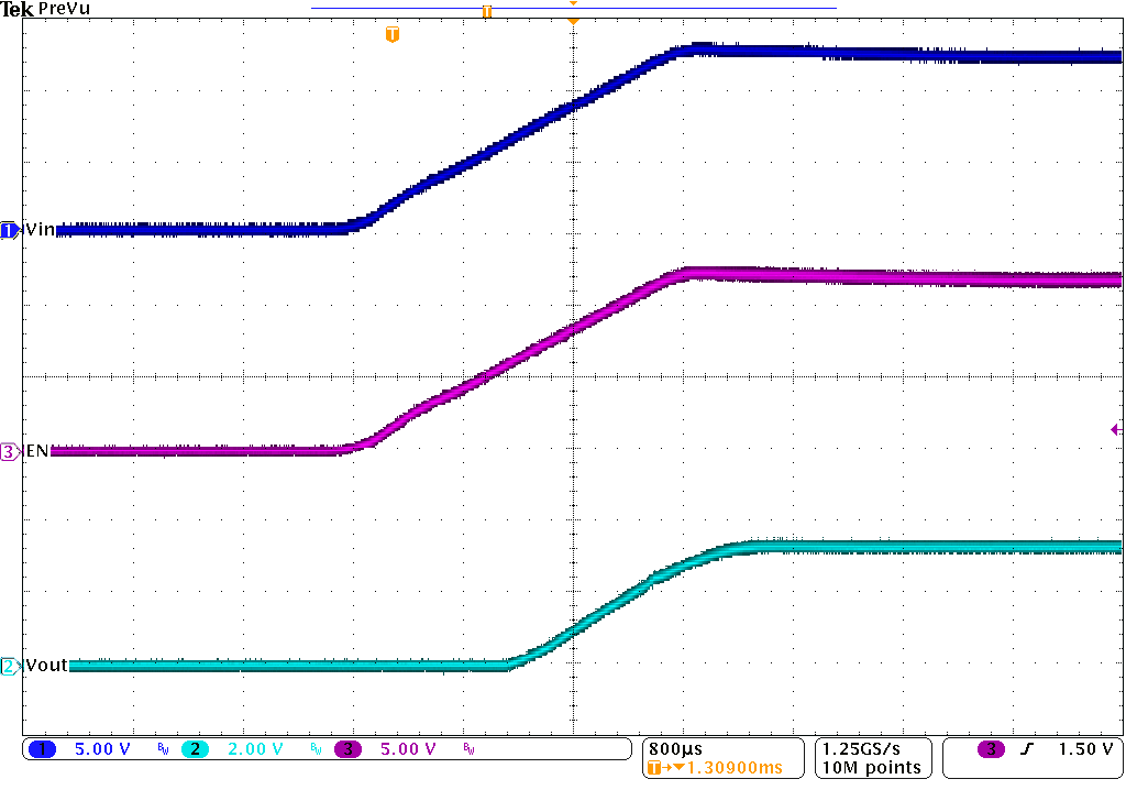
TPS563249 Startup by Vin at 0A_2p0.png
IOUT = 0 A
Figure 26. Start Up Relative to VIN
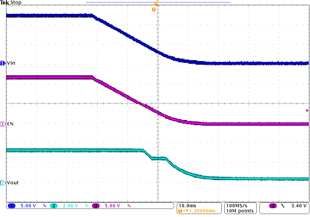
TPS563249 Shutdown by Vin at 0A_2p0.png
IOUT = 0 A
Figure 28. Shutdown Relative to VIN
TPS563249 Vout ripple 0A_2p0.png
IOUT = 0 A
Figure 23. Output Voltage Ripple
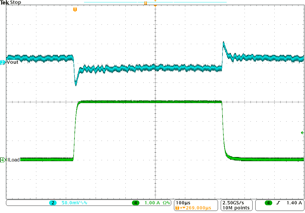
TPS563249 load tran 0to3A 1.6A-us_2p0.png
Slew rate is 1.6 A/µS
Figure 25. Transient Response, 0 to 3 A
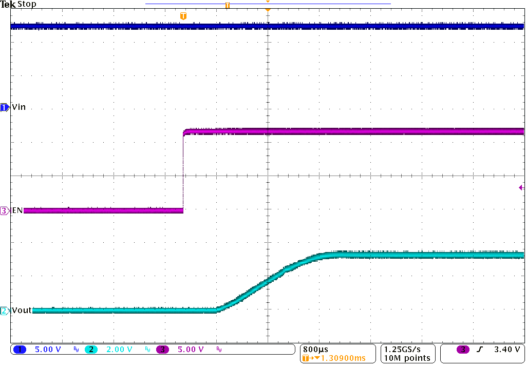
TPS563249 Startup by EN at 3A_2p0.png
IOUT = 3 A
Figure 27. Start-Up Relative to EN
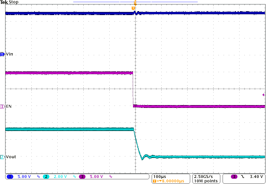
TPS563249 Shutdown by EN at 3A_2p0.png
IOUT = 3 A
Figure 29. Shutdown Relative to EN