ZHCSEL5C December   2015  – April 2024 TPS562201 , TPS562208

PRODUCTION DATA  

  1.   1
  2. 特性
  3. 应用
  4. 说明
  5. Pin Configuration and Functions
  6. Specifications
    1. 5.1 Absolute Maximum Ratings
    2. 5.2 ESD Ratings
    3. 5.3 Recommended Operating Conditions
    4. 5.4 Thermal Information
    5. 5.5 Electrical Characteristics
    6. 5.6 Typical Characteristics
  7. Detailed Description
    1. 6.1 Overview
    2. 6.2 Functional Block Diagram
    3. 6.3 Feature Description
      1. 6.3.1 Adaptive On-Time Control and PWM Operation
      2. 6.3.2 Pulse Skip Control (TPS562201)
      3. 6.3.3 Soft Start and Pre-Biased Soft Start
      4. 6.3.4 Current Protection
      5. 6.3.5 Undervoltage Lockout (UVLO) Protection
      6. 6.3.6 Thermal Shutdown
    4. 6.4 Device Functional Modes
      1. 6.4.1 Normal Operation
      2. 6.4.2 Eco-mode Operation
      3. 6.4.3 Standby Operation
  8. Application and Implementation
    1. 7.1 Application Information
    2. 7.2 Typical Application
      1. 7.2.1 Design Requirements
      2. 7.2.2 Detailed Design Procedure
        1. 7.2.2.1 Custom Design with WEBENCH® Tools
        2. 7.2.2.2 Output Voltage Resistors Selection
        3. 7.2.2.3 Output Filter Selection
        4. 7.2.2.4 Input Capacitor Selection
        5. 7.2.2.5 Bootstrap Capacitor Selection
      3. 7.2.3 Application Curves
    3. 7.3 Power Supply Recommendations
    4. 7.4 Layout
      1. 7.4.1 Layout Guidelines
      2. 7.4.2 Layout Example
  9. Device and Documentation Support
    1. 8.1 Device Support
      1. 8.1.1 Development Support
        1. 8.1.1.1 Custom Design with WEBENCH® Tools
    2. 8.2 接收文档更新通知
    3. 8.3 支持资源
    4. 8.4 Trademarks
    5. 8.5 静电放电警告
    6. 8.6 术语表
  10. Revision History
  11. 10Mechanical, Packaging, and Orderable Information

封装选项

机械数据 (封装 | 引脚)
散热焊盘机械数据 (封装 | 引脚)
订购信息

Application Curves

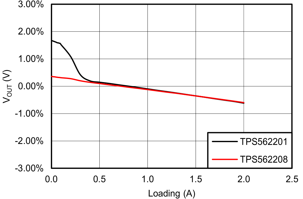
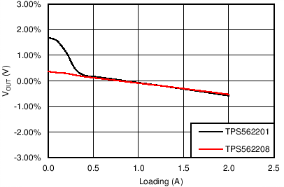
TPS562201 TPS562208 Load
                        Regulation, VIN = 5 VFigure 7-2 Load Regulation, VIN = 5 V
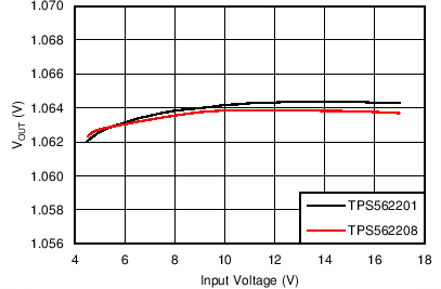
TPS562201 TPS562208 Line
                        Regulation
TPS562201: Iout = 1 A
TPS562208: Iout = 10 mA
Figure 7-4 Line Regulation
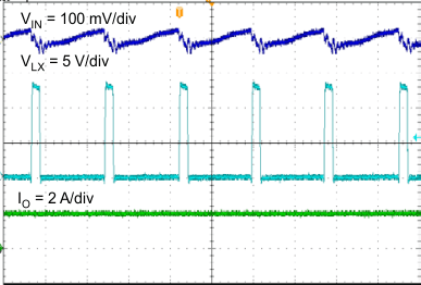
TPS562201 TPS562208 TPS562201 Input Voltage Ripple
800 ns/div
Figure 7-6 TPS562201 Input Voltage Ripple
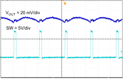
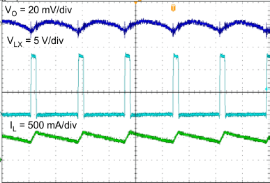
TPS562201 TPS562208 TPS562201 Output Voltage Ripple, IOUT = 0.25 A
1 µs/div
Figure 7-8 TPS562201 Output Voltage Ripple, IOUT = 0.25 A
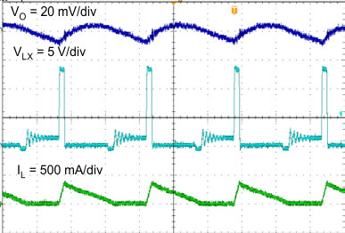
TPS562201 TPS562208 TPS562208 Output Voltage Ripple, IOUT = 0 A
800 ns/div
Figure 7-10 TPS562208 Output Voltage Ripple, IOUT = 0 A
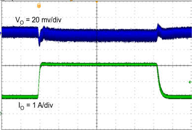
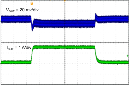
TPS562201 TPS562208 TPS562201 Transient Response, 0.75 to 2.25 A
100 µs/div
Figure 7-12 TPS562201 Transient Response, 0.75 to 2.25 A
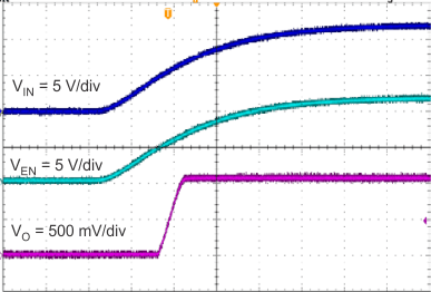
TPS562201 TPS562208 TPS562201 Start-Up Relative to VI
2 ms/div
Figure 7-14 TPS562201 Start-Up Relative to VI
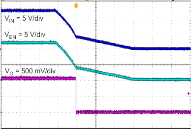
TPS562201 TPS562208 TPS562201 Shutdown Relative to VI
10 ms/div
Figure 7-16 TPS562201 Shutdown Relative to VI
TPS562201 TPS562208 Load
                        Regulation VIN = 12 VFigure 7-3 Load Regulation VIN = 12 V
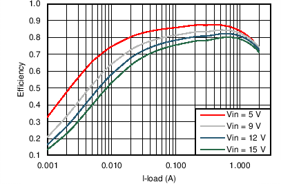
TPS562201 TPS562208 TPS562201 Efficiency, VOUT = 1.05 VFigure 7-5 TPS562201 Efficiency, VOUT = 1.05 V
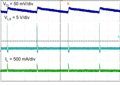
TPS562201 TPS562208 TPS562201 Output Voltage Ripple, IOUT = 10 mA
20 ns/div
Figure 7-7 TPS562201 Output Voltage Ripple, IOUT = 10 mA
TPS562201 TPS562208 TPS562201 Output Voltage Ripple, IOUT = 2 A
1 µs/div
Figure 7-9 TPS562201 Output Voltage Ripple, IOUT = 2 A
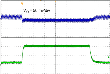
TPS562201 TPS562208 TPS562201 Transient Response, 0.1 to 1.5 A
100 µs/div
Figure 7-11 TPS562201 Transient Response, 0.1 to 1.5 A
TPS562201 TPS562208 TPS562208 Transient Response 0.1 to 2 A
100 µs/div
Figure 7-13 TPS562208 Transient Response 0.1 to 2 A
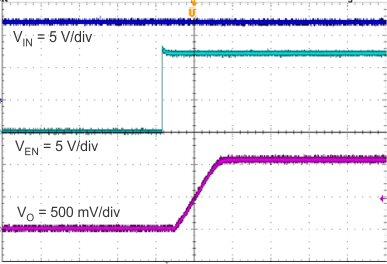
TPS562201 TPS562208 TPS562201 Start-Up Relative to EN
1 ms/div
Figure 7-15 TPS562201 Start-Up Relative to EN
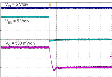
TPS562201 TPS562208 TPS562201 Shutdown Relative to EN
10 µs/div
Figure 7-17 TPS562201 Shutdown Relative to EN