ZHCSC24E january   2014  – may 2023 TPS562200 , TPS563200

PRODUCTION DATA  

  1.   1
  2. 特性
  3. 应用
  4. 说明
  5. Revision History
  6. Pin Configuration and Functions
  7. Specifications
    1. 6.1 Absolute Maximum Ratings #GUID-10807E29-2FD4-4A3F-94B2-FDEBD147A133/SLVSC819633
    2. 6.2 ESD Ratings
    3. 6.3 Recommended Operating Conditions
    4. 6.4 Thermal Information
    5. 6.5 Electrical Characteristics
    6. 6.6 Timing Requirements
    7. 6.7 Typical Characteristics TPS562200
    8. 6.8 Typical Characteristics TPS563200
  8. Detailed Description
    1. 7.1 Overview
    2. 7.2 Functional Block Diagram
    3. 7.3 Feature Description
      1. 7.3.1 The Adaptive On-Time Control And PWM Operation
      2. 7.3.2 Advanced Eco-mode Control
      3. 7.3.3 Soft Start And Pre-Biased Soft Start
      4. 7.3.4 Current Protection
      5. 7.3.5 Over Voltage Protection
      6. 7.3.6 UVLO Protection
      7. 7.3.7 Thermal Shutdown
    4. 7.4 Device Functional Modes
      1. 7.4.1 Normal Operation
      2. 7.4.2 Eco-mode Operation
      3. 7.4.3 Standby Operation
  9. Application and Implementation
    1. 8.1 Application Information
    2. 8.2 Typical Applications
      1. 8.2.1 Tps562200 4.5-V To 17-V Input, 1.05-V Output Converter
        1. 8.2.1.1 Design Requirements
        2. 8.2.1.2 Detailed Design Procedures
          1. 8.2.1.2.1 Custom Design with WEBENCH® Tools
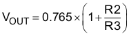
          2. 8.2.1.2.2 Output Voltage Resistors Selection
          3. 8.2.1.2.3 Output Filter Selection
          4. 8.2.1.2.4 Input Capacitor Selection
          5. 8.2.1.2.5 Bootstrap Capacitor Selection
        3. 8.2.1.3 Application Curves
      2. 8.2.2 Tps563200 4.5-V To 17-V Input, 1.05-V Output Converter
        1. 8.2.2.1 Design Requirements
        2. 8.2.2.2 Detailed Design Procedures
          1. 8.2.2.2.1 Output Filter Selection
        3. 8.2.2.3 Application Curves
    3. 8.3 Power Supply Recommendations
    4. 8.4 Layout
      1. 8.4.1 Layout Guidelines
      2. 8.4.2 Layout Example
  10. Device and Documentation Support
    1. 9.1 Device Support
      1. 9.1.1 Development Support
        1. 9.1.1.1 Custom Design with WEBENCH® Tools
    2. 9.2 接收文档更新通知
    3. 9.3 支持资源
    4. 9.4 Trademarks
    5. 9.5 静电放电警告
    6. 9.6 术语表
  11. 10Mechanical, Packaging, And Orderable Information

封装选项

机械数据 (封装 | 引脚)
散热焊盘机械数据 (封装 | 引脚)
订购信息
Output Voltage Resistors Selection

The output voltage is set with a resistor divider from the output node to the VFB pin. TI recommends to use 1% tolerance or better divider resistors. Start by using Equation 2 to calculate VOUT.

To improve efficiency at light loads consider using larger value resistors, too high of resistance is more susceptible to noise and voltage errors from the VFB input current are more noticeable.

Equation 2. GUID-18566819-89B8-4AA9-9A98-04377A7775C4-low.gif