ZHCSBE2A August 2013 – October 2022 TPS54625
PRODUCTION DATA
- 1 特性
- 2 应用范围
- 3 说明
- 4 ORDERING INFORMATION (1)
- 5 最大绝对额定值
- 6 THERMAL INFORMATION
- 7 RECOMMENDED OPERATING CONDITIONS
- 8 ELECTRICAL CHARACTERISTICS
- 9 DEVICE INFORMATION
- 10OVERVIEW
- 11DETAILED DESCRIPTION
- 12TYPICAL CHARACTERISTICS
- 13DESIGN GUIDE
- 14THERMAL INFORMATION
- 15LAYOUT CONSIDERATIONS
- 16Revision History
9 DEVICE INFORMATION
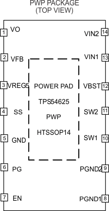
Pin Functions
| PIN | DESCRIPTION | |
|---|---|---|
| NAME | NUMBER | |
| VO | 1 | Connect to output of converter. This pin is used for output discharge function. |
| VFB | 2 | Converter feedback input. Connect with feedback resistor divider. |
| VREG5 | 3 | 5.5V power supply output. An external capacitor (typical 1uF) should be connected to GND. VREG5 is not active when EN is low. |
| SS | 4 | Soft start control. An external capacitor should be connected to GND. |
| GND | 5 | Signal ground pin. |
| PG | 6 | Open drain power good output |
| EN | 7 | Enable control input. EN is active high and must be pulled up to enable the device. |
| PGND1, PGND2 | 8, 9 | Ground returns for low-side MOSFET. Also serve as inputs of current comparators. Connect PGND and GND strongly together near the IC. |
| SW1,SW2 | 10, 11 | Switch node connection between high-side NFET and low-side NFET. Also serve as inputs to current comparator. |
| VBST | 12 | Supply input for high-side NFET gate driver (boost terminal). Connect capacitor from this pin to respective SW1, SW2 terminals. An internal PN diode is connected between VREG5 and VBST pin. |
| VIN1, VIN2 | 13, 14 | Power Input and connected to high side NFET drain. Supply Input for 5V internal linear regulator for the control circuitry |
| PowerPAD™ | Back side | Thermal pad of the package. Must be soldered to achieve appropriate dissipation. Should be connected to PGND |
") Figure 9-1 FUNCTIONAL BLOCK DIAGRAM
(HTSSOP)
Figure 9-1 FUNCTIONAL BLOCK DIAGRAM
(HTSSOP)