ZHCSJY4B July   2008  – June 2019 TPS5450-Q1

PRODUCTION DATA.  

  1. 特性
  2. 应用
  3. 说明
    1.     Device Images
      1.      简化原理图和效率曲线
  4. 修订历史记录
  5. Pin Configuration and Functions
    1.     Pin Functions
  6. Specifications
    1. 6.1 Absolute Maximum Ratings
    2. 6.2 Recommended Operating Conditions
    3. 6.3 Thermal Information
    4. 6.4 Dissipation Ratings
    5. 6.5 Electrical Characteristics
    6. 6.6 Typical Characteristics
  7. Detailed Description
    1. 7.1 Overview
    2. 7.2 Functional Block Diagram
    3. 7.3 Feature Description
      1. 7.3.1  Oscillator Frequency
      2. 7.3.2  Voltage Reference
      3. 7.3.3  Enable (ENA) and Internal Slow Start
      4. 7.3.4  Undervoltage Lockout (UVLO)
      5. 7.3.5  Output Feedback (VSENSE) and Internal Compensation
      6. 7.3.6  Voltage Feedforward
      7. 7.3.7  Pulse-Width-Modulation (PWM) Control
      8. 7.3.8  Overcurrent Limiting
      9. 7.3.9  Overvoltage Protection
      10. 7.3.10 Thermal Shutdown
  8. Application Information
    1. 8.1 Application Information
    2. 8.2 Typical Application
      1. 8.2.1 Design Requirements
      2. 8.2.2 Detailed Design Procedure
        1. 8.2.2.1  Custom Design With WEBENCH® Tools
        2. 8.2.2.2  Boost Capacitor (BOOT)
        3. 8.2.2.3  Switching Frequency
        4. 8.2.2.4  Input Capacitors
        5. 8.2.2.5  Output Filter Components
          1. 8.2.2.5.1 Inductor Selection
          2. 8.2.2.5.2 Capacitor Selection
        6. 8.2.2.6  Output Voltage Setpoint
        7. 8.2.2.7  Boot Capacitor
        8. 8.2.2.8  Catch Diode
        9. 8.2.2.9  Output Voltage Limitations
        10. 8.2.2.10 Internal Compensation Network
      3. 8.2.3 Application Curves
  9. Layout
    1. 9.1 Layout Guidelines
    2. 9.2 Layout Examples
    3. 9.3 Thermal Calculations
  10. 10器件和文档支持
    1. 10.1 器件支持
      1. 10.1.1 第三方产品免责声明
    2. 10.2 开发支持
      1. 10.2.1 使用 WEBENCH® 工具创建定制设计
    3. 10.3 接收文档更新通知
    4. 10.4 社区资源
    5. 10.5 商标
    6. 10.6 静电放电警告
    7. 10.7 Glossary
  11. 11机械、封装和可订购信息

封装选项

机械数据 (封装 | 引脚)
散热焊盘机械数据 (封装 | 引脚)
订购信息

Application Curves

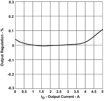
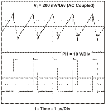
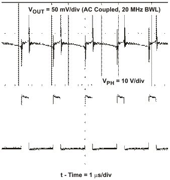
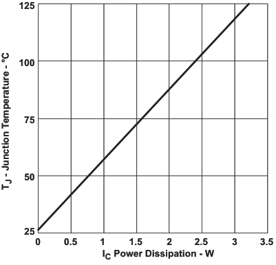
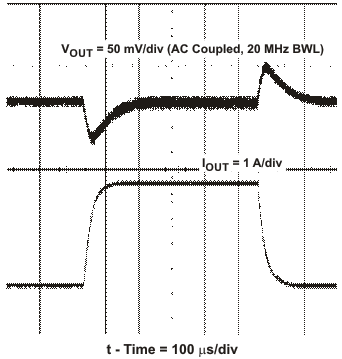
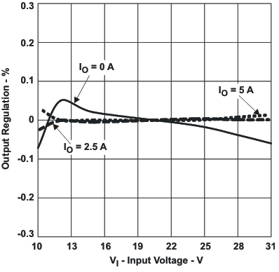
The performance graphs (Figure 10 through Figure 16) are applicable to the circuit in Figure 9. TA = 25 °C. unless otherwise specified.
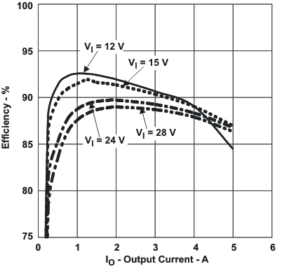
TPS5450-Q1 eff2_io_lvs757.gif
Figure 10. Efficiency vs Output Current
TPS5450-Q1 lr_vi_lvs757.gif
Figure 12. Output Regulation % vs Input Voltage
TPS5450-Q1 lr_io_lvs757.gif
Figure 11. Output Regulation % vs Output Current
TPS5450-Q1 iripp_lvs757.gif
IOUT = 5 A
Figure 13. Input Voltage Ripple and PH Node
TPS5450-Q1 out_ripp_lvs632.gif
IOUT = 5 A
Figure 14. Output Voltage Ripple and PH Node
TPS5450-Q1 pd_v_jtemp_lvs757.gif
Figure 16. TPS5450-Q1 Power Dissipation vs Junction Temperature.
TPS5450-Q1 trans_lvs632.gif
IOUT Step 1.25 To 3.75 A
Figure 15. Transient Response