ZHCSEL6D November 2014 – February 2016 TPS54335-1A , TPS54335A , TPS54336A
PRODUCTION DATA.
- 1 特性
- 2 应用范围
- 3 说明
- 4 修订历史记录
- 5 Pin Configuration and Functions
- 6 Specifications
-
7 Detailed Description
- 7.1 Overview
- 7.2 Functional Block Diagram
- 7.3
Feature Description
- 7.3.1 Fixed-Frequency PWM Control
- 7.3.2 Light-Load Operation
- 7.3.3 Voltage Reference
- 7.3.4 Adjusting the Output Voltage
- 7.3.5 Enabling and Adjusting Undervoltage Lockout
- 7.3.6 Error Amplifier
- 7.3.7 Slope Compensation and Output Current
- 7.3.8 Safe Startup into Pre-Biased Outputs
- 7.3.9 Bootstrap Voltage (BOOT)
- 7.3.10 Adjustable Switching Frequency (TPS54335A Only)
- 7.3.11 Soft-Start (TPS54336A Only)
- 7.3.12 Output Overvoltage Protection (OVP)
- 7.3.13 Overcurrent Protection
- 7.3.14 Thermal Shutdown
- 7.3.15 Small-Signal Model for Loop Response
- 7.3.16 Simple Small-Signal Model for Peak Current-Mode Control
- 7.3.17 Small-Signal Model for Frequency Compensation
- 7.4 Device Functional Modes
-
8 Application and Implementation
- 8.1 Application Information
- 8.2
Typical Applications
- 8.2.1
TPS5433xA and TPS54335-1A Family Application
- 8.2.1.1 Design Requirements
- 8.2.1.2 Detailed Design Procedure
- 8.2.1.3 Application Curves
- 8.2.2 TPS54336A Typical Application
- 8.2.1
TPS5433xA and TPS54335-1A Family Application
- 9 Power Supply Recommendations
- 10Layout
- 11器件和文档支持
- 12机械、封装和可订购信息
封装选项
请参考 PDF 数据表获取器件具体的封装图。
机械数据 (封装 | 引脚)
- DRC|10
- DDA|8
散热焊盘机械数据 (封装 | 引脚)
订购信息
5 Pin Configuration and Functions
DDA Package
8-Pin SO PowerPAD
TPS54335A Top View

DDA Package
8-Pin SO PowerPAD
TPS54336A Top View

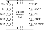
DRC Package
10-Pin VSON With Exposed Thermal Pad
TPS54335A and TPS54335-1A Top View

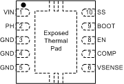
DRC Package
10-Pin VSON With Exposed Thermal Pad
TPS54336A Top View

Pin Functions
| PIN | I/O | DESCRIPTION | ||
|---|---|---|---|---|
| NAME | SO PowerPAD | VSON | ||
| BOOT | 1 | 9 | O | A bootstrap capacitor is required between the BOOT and PH pins. If the voltage on this capacitor is below the minimum required by the output device, the output is forced to switch off until the capacitor is refreshed. |
| COMP | 6 | 7 | O | This pin is the error-amplifier output and the input to the output switch-current comparator. Connect frequency compensation components to this pin. |
| EN | 7 | 8 | I | This pin is the enable pin. Float the EN pin to enable. |
| GND | 4 | 3 | — | Ground |
| 4 | ||||
| 5 | ||||
| PH | 3 | 2 | O | The PH pin is the source of the internal high-side power MOSFET. |
| RT (TPS54335A and TPS54335-1A) | 8 | 10 | O | Connect the RT pin to an external timing resistor to adjust the switching frequency of the device. |
| SS (TPS54336A) | The SS pin is the soft-start and tracking pin. An external capacitor connected to this pin sets the internal voltage-reference rise time. The voltage on this pin overrides the internal reference. | |||
| VIN | 2 | 1 | — | This pin is the 4.5- to 28-V input supply voltage. |
| VSENSE | 5 | 6 | I | This pin is the inverting node of the transconductance (gm) error amplifier. |
| PowerPAD (SO only) | — | For proper operation, connect the GND pin to the exposed thermal pad. This thermal pad should be connected to any internal PCB ground plane using multiple vias for good thermal performance. | ||
| Thermal pad (VSON only) | ||||