SLVS876D November 2008 – November 2014 TPS54232
PRODUCTION DATA.
- 1 Features
- 2 Applications
- 3 Description
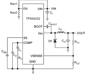
- 4 Simplified Schematic
- 5 Revision History
- 6 Pin Configuration and Functions
- 7 Specifications
-
8 Detailed Description
- 8.1 Overview
- 8.2 Functional Block Diagram
- 8.3
Feature Description
- 8.3.1 Fixed-Frequency PWM Control
- 8.3.2 Voltage Reference (Vref)
- 8.3.3 Bootstrap Voltage (BOOT)
- 8.3.4 Enable and Adjustable Input Undervoltage Lockout (VIN UVLO)
- 8.3.5 Programmable Slow-Start Using SS Pin
- 8.3.6 Error Amplifier
- 8.3.7 Slope Compensation
- 8.3.8 Current Mode Compensation Design
- 8.3.9 Overcurrent Protection and Frequency Shift
- 8.3.10 Overvoltage Transient Protection
- 8.3.11 Thermal Shutdown
- 8.4 Device Functional Modes
-
9 Application and Implementation
- 9.1 Application Information
- 9.2
Typical Application
- 9.2.1 Design Requirements
- 9.2.2 Detailed Design Procedure
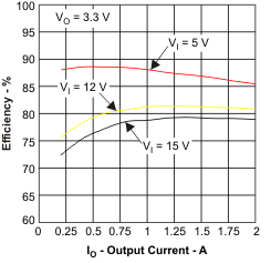
- 9.2.3 Application Curves
- 10Power Supply Recommendations
- 11Layout
- 12Device And Documentation Support
- 13Mechanical, Packaging, And Orderable Information
1 Features
- 3.5-V to 28-V Input Voltage Range
- Adjustable Output Voltage Down to 0.8 V
- Integrated 80-mΩ High-Side MOSFET Supports up to 2-A Continuous Output Current
- High Efficiency at Light Loads with a Pulse-Skipping Eco-Mode™
- Fixed 1-MHz Switching Frequency
- Typical 1-μA Shutdown Quiescent Current
- Adjustable Slow-Start Limits Inrush Currents
- Programmable UVLO Threshold
- Overvoltage Transient Protection
- Cycle-by-Cycle Current Limit, Frequency Fold Back and Thermal Shutdown Protection
- Available in 8-Pin SOIC Package
- Supported by WEBENCH® Software Tool (http://www.ti.com/lsds/ti/analog/webench/overview.page)
2 Applications
- Consumer Applications such as Set-Top Boxes, CPE Equipment, LCD Displays, Peripherals, and Battery Chargers
- Industrial and Car Audio Power Supplies
- 5-V, 12-V, and 24-V Distributed Power Systems
3 Description
The TPS54232 is a 28-V, nonsynchronous buck converter that integrates a low RDS(on) high-side MOSFET. To increase efficiency at light loads, a pulse-skipping Eco-Mode feature is automatically activated. Furthermore, the 1-μA shutdown supply current allows the device to be used in battery-powered applications. Current mode control with internal slope compensation simplifies the external compensation calculations and reduces component count while allowing the use of ceramic output capacitors. A resistor divider programs the hysteresis of the input undervoltage lockout. An overvoltage transient protection circuit limits voltage overshoots during startup and transient conditions. A cycle-by-cycle current limit scheme, frequency fold back, and thermal shutdown protect the device and the load in the event of an overload condition. The TPS54232 is available in an 8-pin SOIC package.
Device Information(1)
| PART NUMBER | PACKAGE | BODY SIZE (NOM) |
|---|---|---|
| TPS54232 | SOIC (8) | 4.90 mm x 3.90 mm |
- For all available packages, see the orderable addendum at the end of the datasheet.
4 Simplified Schematic
Efficiency