SLUSA68A December   2010  – October 2016 TPS53310

PRODUCTION DATA.  

  1. Features
  2. Applications
  3. Description
  4. Revision History
  5. Pin Configuration and Functions
  6. Specifications
    1. 6.1 Absolute Maximum Ratings
    2. 6.2 ESD Ratings
    3. 6.3 Recommended Operating Conditions
    4. 6.4 Thermal Information
    5. 6.5 Electrical Characteristics
    6. 6.6 Typical Characteristics
  7. Detailed Description
    1. 7.1 Overview
    2. 7.2 Functional Block Diagram
    3. 7.3 Feature Description
      1. 7.3.1 Soft Start
      2. 7.3.2 Power Good
      3. 7.3.3 Undervoltage Lockout (UVLO) Function
      4. 7.3.4 Overcurrent Protection
      5. 7.3.5 Overvoltage Protection
      6. 7.3.6 Undervoltage Protection
      7. 7.3.7 Overtemperature Protection
      8. 7.3.8 Output Discharge
    4. 7.4 Device Functional Modes
      1. 7.4.1 Operation Mode
      2. 7.4.2 Eco-mode™ Light-Load Operation
      3. 7.4.3 Forced Continuous Conduction Mode (FCCM)
    5. 7.5 Programming
      1. 7.5.1 Master/Slave Operation and Synchronization
  8. Application and Implementation
    1. 8.1 Application Information
    2. 8.2 Typical Application
      1. 8.2.1 Design Requirements
      2. 8.2.2 Detailed Design Procedure
        1. 8.2.2.1 Determine the Value of R1 and R2
        2. 8.2.2.2 Choose the Inductor
        3. 8.2.2.3 Choose the Output Capacitor(s)
        4. 8.2.2.4 Choose the Input Capacitor
        5. 8.2.2.5 Compensation Design
      3. 8.2.3 Application Curves
  9. Power Supply Recommendations
  10. 10Layout
    1. 10.1 Layout Guidelines
    2. 10.2 Layout Example
  11. 11Device and Documentation Support
    1. 11.1 Documentation Support
      1. 11.1.1 Related Documentation
    2. 11.2 Receiving Notification of Documentation Updates
    3. 11.3 Community Resources
    4. 11.4 Trademarks
    5. 11.5 Electrostatic Discharge Caution
    6. 11.6 Glossary
  12. 12Mechanical, Packaging, and Orderable Information

封装选项

机械数据 (封装 | 引脚)
散热焊盘机械数据 (封装 | 引脚)
订购信息

Layout

Layout Guidelines

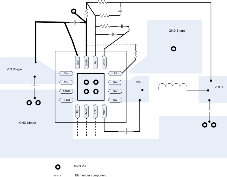
Good layout is essential for stable power supply operation. Follow these guidelines for a clean PCB layout:

  • Separate the power ground and analog ground planes. Connect them together at one location.
  • Use four vias to connect the thermal pad to power ground.
  • Place VIN and VDD decoupling capacitors as close to the device as possible.
  • Use wide traces for VIN, VOUT, PGND and SW. These nodes carry high current and also serve as heat sinks.
  • Place feedback and compensation components as close to the device as possible.
  • Keep analog signals (FB, COMP) away from noisy signals (SW, SYNC, VBST).
  • See TPS53310 evaluation module, Using the TPS53310EVM-755, A 3-A Eco-mode™ Integrated Switcher With Master-Slave (SLUU826), for a detailed layout example.

Layout Example

TPS53310 v10214_lusaf3.gif Figure 27. TPS53310 Layout Example