ZHCSI35C November   2009  – April 2018 TPS51200-Q1

PRODUCTION DATA.  

  1. 特性
  2. 应用
  3. 说明
    1.     Device Images
      1.      标准 DDR 应用
  4. 修订历史记录
  5. Pin Configuration and Functions
    1.     Pin Functions
  6. Specifications
    1. 6.1 Absolute Maximum Ratings
    2. 6.2 ESD Ratings
    3. 6.3 Recommended Operating Conditions
    4. 6.4 Thermal Information
    5. 6.5 Electrical Characteristics
    6. 6.6 Switching Characteristics
    7. 6.7 Typical Characteristics
  7. Detailed Description
    1. 7.1 Overview
    2. 7.2 Functional Block Diagram
    3. 7.3 Feature Description
      1. 7.3.1 Sink and Source Regulator (VO Pin)
      2. 7.3.2 Reference Input (REFIN Pin)
      3. 7.3.3 Reference Output (REFOUT Pin)
      4. 7.3.4 Soft-Start Sequencing
      5. 7.3.5 Enable Control (EN Pin)
      6. 7.3.6 Powergood Function (PGOOD Pin)
      7. 7.3.7 Current Protection (VO Pin)
      8. 7.3.8 UVLO Protection (VIN Pin)
      9. 7.3.9 Thermal Shutdown
    4. 7.4 Device Functional Modes
      1. 7.4.1 S3 and Pseudo-S5 Support
      2. 7.4.2 Tracking Startup and Shutdown
  8. Application and Implementation
    1. 8.1 Application Information
    2. 8.2 Typical Application
      1. 8.2.1 VTT DIMM Applications
        1. 8.2.1.1 Design Parameters
        2. 8.2.1.2 Detailed Design Procedure
          1. 8.2.1.2.1 VIN Capacitor
          2. 8.2.1.2.2 VLDO Input Capacitor
          3. 8.2.1.2.3 Output Capacitor
          4. 8.2.1.2.4 Output Tolerance Consideration for VTT DIMM Applications
        3. 8.2.1.3 Application Curves
      2. 8.2.2 Design Example 1
        1. 8.2.2.1 Design Parameters
      3. 8.2.3 Design Example 2
        1. 8.2.3.1 Design Parameters
      4. 8.2.4 Design Example 3
        1. 8.2.4.1 Design Parameters
      5. 8.2.5 Design Example 4
        1. 8.2.5.1 Design Parameters
      6. 8.2.6 Design Example 5
        1. 8.2.6.1 Design Parameters
      7. 8.2.7 Design Example 6
        1. 8.2.7.1 Design Parameters
      8. 8.2.8 Design Example 7
        1. 8.2.8.1 Design Parameters
  9. Power Supply Recommendations
  10. 10Layout
    1. 10.1 Layout Guidelines
    2. 10.2 Layout Example
    3. 10.3 Thermal Considerations
  11. 11器件和文档支持
    1. 11.1 器件支持
      1. 11.1.1 Third-Party Products Disclaimer
    2. 11.2 文档支持
      1. 11.2.1 相关文档
    3. 11.3 接收文档更新通知
    4. 11.4 社区资源
    5. 11.5 商标
    6. 11.6 静电放电警告
    7. 11.7 Glossary
  12. 12机械、封装和可订购信息

封装选项

机械数据 (封装 | 引脚)
散热焊盘机械数据 (封装 | 引脚)
订购信息

Typical Characteristics

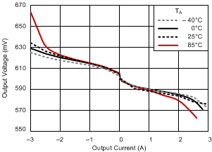
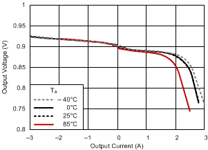
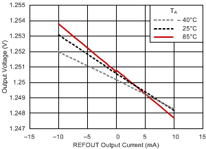
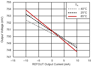
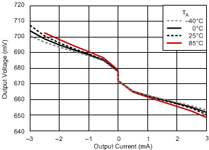
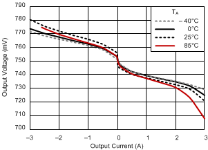
For Figure 1 through Figure 18, 3 × 10-μF MLCCs (0805) are used on the output.
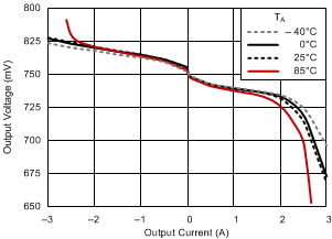
TPS51200-Q1 load_reg_ddr_33_slus812.gif
VVIN = 3.3 V DDR
Figure 1. Output Voltage vs Output Current
TPS51200-Q1 load_reg_ddr3_33_slus812.gif
VVIN = 3.3 V DDR3
Figure 3. Output Voltage vs Output Current
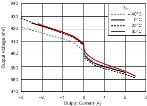
TPS51200-Q1 load_reg_lpddr3_33_slus812.gif
VVIN = 3.3 V LP DDR3 or DDR4
Figure 5. Output Voltage vs Output Current
TPS51200-Q1 load_reg_ddr2_25_slus812.gif
VVIN = 2.5 V DDR2
Figure 7. Output Voltage vs Output Current
TPS51200-Q1 load_reg_ddr3l_25_slus812.gif
VVIN = 2.5 V DDR3L
Figure 9. Output Voltage vs Output Current
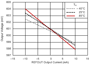
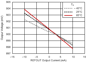
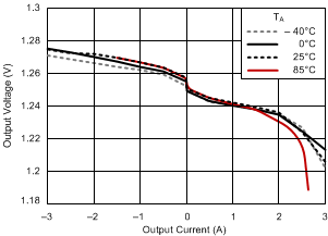
TPS51200-Q1 refout_load_reg_ddr_slus812.gif
DDR
Figure 11. REFOUT Line Regulation
TPS51200-Q1 refout_load_reg_ddr3_slus812.gif
DDR3
Figure 13. REFOUT Line Regulation
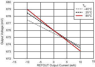
TPS51200-Q1 refout_load_reg_lpddr3_slus812.gif
LP DDR3 or DDR4
Figure 15. REFOUT Line Regulation
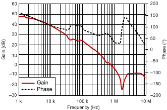
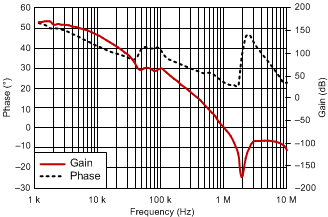
TPS51200-Q1 bode_ddr2_slus812.gif
DDR2
Figure 17. Gain and Phase vs Frequency
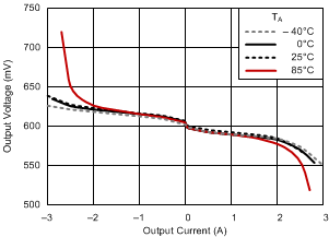
TPS51200-Q1 load_reg_ddr2_33_slus812.gif
VVIN = 3.3 V DDR2
Figure 2. Output Voltage vs Output Current
TPS51200-Q1 load_reg_ddr3l_33_slus812.gif
VVIN = 3.3 V DDR3L
Figure 4. Output Voltage vs Output Current
TPS51200-Q1 load_reg_ddr_25_slus812.gif
VVIN =2.5 V DDR
Figure 6. Output Voltage vs Output Current
TPS51200-Q1 load_reg_ddr3_25_slus812.gif
VVIN = 2.5 V DDR3
Figure 8. Output Voltage vs Output Current
TPS51200-Q1 load_reg_lpddr3_25_slus812.gif
VVIN = 2.5 V LP DDR3 or DDR4
Figure 10. Output Voltage vs Output Current
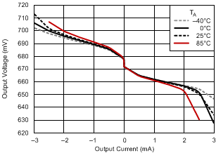
TPS51200-Q1 refout_load_reg_ddr2_slus812.gif
DDR2
Figure 12. REFOUT Line Regulation
TPS51200-Q1 refout_load_reg_ddr3l_slus812.gif
DDR3L
Figure 14. REFOUT Line Regulation
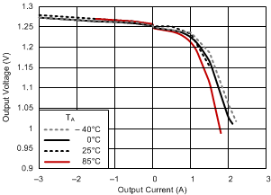
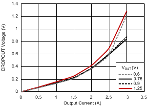
TPS51200-Q1 droupout_reg_slus812.gif
Figure 16. DROPOUT Voltage vs Output Current
TPS51200-Q1 bode_ddr3_slus812.gif
DDR3
Figure 18. Gain and Phase vs Frequency