SLUS670C JULY 2005 – January 2015 TPS51120
PRODUCTION DATA.
- 1 Features
- 2 Applications
- 3 Description
- 4 Revision History
- 5 Pin Configuration and Functions
- 6 Specifications
-
7 Detailed Description
- 7.1 Overview
- 7.2 Functional Block Diagram
- 7.3
Feature Description
- 7.3.1 PWM Operation
- 7.3.2 Adaptive On-Time Control
- 7.3.3 Light Load Operation
- 7.3.4 Forced PWM Operation
- 7.3.5 5-V, 100-mA, LDO and Switchover (VREG5)
- 7.3.6 3.3-V, 100-mA, LDO and Switchover (VREG3)
- 7.3.7 2-V, 50-uA Sink - Source Reference (VREF2)
- 7.3.8 Low-Side Driver
- 7.3.9 High-Side Driver
- 7.3.10 Soft-Start
- 7.3.11 Soft-Stop
- 7.3.12 Powergood
- 7.3.13 Current Sensing and Overcurrent Protection
- 7.3.14 Overvoltage Protection
- 7.3.15 Undervoltage Protection
- 7.3.16 5-V Supply and UVLO Protection
- 7.3.17 VIN Line Sag Protection (Dynamic UVP)
- 7.3.18 Thermal Shutdown
- 7.4 Device Functional Modes
- 7.5 Programming
- 8 Application and Implementation
- 9 Power Supply Recommendations
- 10Layout
- 11Device and Documentation Support
- 12Mechanical, Packaging, and Orderable Information
封装选项
请参考 PDF 数据表获取器件具体的封装图。
机械数据 (封装 | 引脚)
- RHB|32
散热焊盘机械数据 (封装 | 引脚)
- RHB|32
订购信息
6 Specifications
6.1 Absolute Maximum Ratings
over operating free-air temperature range unless otherwise noted(1)| MIN | MAX | UNIT | |||
|---|---|---|---|---|---|
| Input voltage | VBST1, VBST2 | –0.3 | 36 | V | |
| VBST1, VBST2 wrt LL | –0.3 | 6 | |||
| VIN, EN5 | –0.3 | 30 | |||
| SKIPSEL, TONSEL, EN1, EN2, CS1, CS2, V5FILT, VFB1, VFB2, EN3, VO1, VO2 | –0.3 | 6 | |||
| Output voltage | DRVH1, DRVH2 | –1 | 36 | V | |
| DRVH1, DRVH2 (wrt LL) | –0.3 | 6 | |||
| LL1, LL2 | –1 | 30 | |||
| VREF2, VREG3, VREG5, PGOOD1, PGOOD2, DRVL1, DRVL2, COMP1, COMP2 | –0.3 | 6 | |||
| PGND1, PGND2 | –0.3 | 0.3 | |||
| Source/sink current | VREF2 | 1 | mA | ||
| VBST | 100 | ||||
| VREG5, VREG3 (source only) | 200 | ||||
| TA | Operating ambient temperature | –40 | 85 | °C | |
| TJ | Junction temperature | –40 | 125 | ||
| Lead temperature 1.6 mm (1/16 inch) from case for 10 seconds | 255 | ||||
| Tstg | Storage temperature | –55 | 150 | ||
(1) Stresses beyond those listed under Absolute Maximum Ratings may cause permanent damage to the device. These are stress ratings only, and functional operation of the device at these or any other conditions beyond those indicated under Recommended Operating Conditions is not implied. Exposure to absolute-maximum-rated conditions for extended periods may affect device reliability. All voltage values are with respect to the network ground terminal unless otherwise noted.
6.2 Recommended Operating Conditions
| MIN | MAX | UNIT | ||
|---|---|---|---|---|
| Input voltage, V5FILT | 4.5 | 5.5 | V | |
| Input voltage range | VBST1, VBST2 | -0.1 | 34 | V |
| VBST1, VBST2 wrt LL | -0.1 | 5.5 | ||
| VIN, EN5 | -0.1 | 28 | ||
| SKIPSEL, TONSEL, EN1, EN2, CS1, CS2, V5FILT, VFB1, VFB2, EN3 | -0.1 | 5.5 | ||
| VO1, VO2 | -0.1 | 5.5 | ||
| Output voltage range | DRVH1, DRVH2 | -0.8 | 34 | V |
| DRVH1, DRVH2 (wrt LL) | -0.1 | 5.5 | ||
| LL1, LL2 | -0.8 | 28 | ||
| VREF2, VREG5, VREG3, PGOOD1, PGOOD2, DRVL1, DRVL2, COMP1, COMP2 | -0.1 | 5.5 | ||
| PGND1, PGND2 | -0.1 | 0.1 | ||
| Source/sink current | VREF2 | 0.08 | mA | |
| VBST | 50 | |||
| VREG5, VREF3 (source only) | 100 | |||
| Operating ambient temperature range, TA | -40 | 85 | °C | |
6.3 Thermal Information
| THERMAL METRIC(1) | TPS51120 | UNIT | |
|---|---|---|---|
| RHB | |||
| 32 PINS | |||
| RθJA | Junction-to-ambient thermal resistance | 38.5 | °C/W |
(1) For more information about traditional and new thermal metrics, see the IC Package Thermal Metrics application report, SPRA953.
6.4 Electrical Characteristics
over operating free-air temperature range, VVIN = 12 V, VVREG5 = VV5FILT = 5 V (unless otherwise noted)| PARAMETER | TEST CONDITIONS | MIN | TYP | MAX | UNIT | ||
|---|---|---|---|---|---|---|---|
| SUPPLY CURRENT | |||||||
| IINCCAP | Supply current | VIN current, VREG5=VREG3=No Load, EN3=EN5=FLOAT, EN1=EN2=5V, CS=5V, COMP connected to Cap | Current mode | 750 | 1500 | μA | |
| IINNOCAP | Supply current | VIN current, VREG5=VREG3=No Load, EN3=EN5=FLOAT; EN1=EN2=5V, CS=5V, COMP=5V | D-CAP mode | 700 | 1400 | ||
| IIN5(STBY) | Stand-by current | VIN current, VREG5=No Load EN3=0V, EN5=FLOAT, EN1=EN2=0 | 5-V only | 30 | 45 | ||
| IIN3(STBY) | Stand-by current | VIN current, VREG3=No Load EN3=FLOAT, EN5=0, EN1=EN2=0 | 3.3-V only | 12 | 20 | ||
| IIN532(STBY) | Stand-by current | VIN current, VREG5=VREG3=VREF2=No Load EN3=EN5=FLOAT, EN1=EN2=0 | 100 | 160 | |||
| IIN(SHDN) | Shut down current | VIN current, EN3=EN5=EN1=EN2=0V | 10 | 20 | |||
| VOUT and VREF2 VOLTAGES | |||||||
| VOUT | Output voltage | VFB2 = 3.3 V, TA= 25°C, No Load | 3.241 | 3.300 | 3.359 | V | |
| VFB2 = 3.3 V, TA= 0 to 85°C, No Load | 3.234 | 3.300 | 3.366 | ||||
| VFB2 = 3.3 V, TA= -40 to 85°C, No Load | 3.224 | 3.300 | 3.376 | ||||
| VFB1 = 5 V, TA= 25°C, No Load | 4.910 | 5.000 | 5.090 | ||||
| VFB1 = 5 V, TA= 0 to 85°C, No Load | 4.900 | 5.000 | 5.100 | ||||
| VFB1 = 5 V, TA= -40 to 85°C, No Load | 4.885 | 5.000 | 5.115 | ||||
| Adjustable mode output range | 1.0 | 5.5 | |||||
| VADJ | Output regulation voltage | Adjustable mode | 1.00 | V | |||
| VADJ T | Output regulation voltage tolerance | Adjustable mode, TA= 25°C | -0.9% | 0.9% | |||
| Adjustable mode, TA= 0 to 85°C | -1.3% | 1.3% | |||||
| Adjustable mode, TA= -40 to 85°C | -1.6% | 1.6% | |||||
| VVREF2 | 2-V output regulation voltage | IVREF2 ± 50 μA, TA= 25°C | 1.97 | 2.00 | 2.03 | V | |
| VVREF2T | 2-V output regulation voltage tolerance | IVREF2 ± 50 μA, TA= 0 to 85°C | 1.96 | 2.04 | |||
| IVREF2 ± 50 μA, TA= -40 to 85°C | 1.95 | 2.05 | |||||
| IVFB | VFB input current | VFBx=1.02V, COMPx=open | 0.02 | μA | |||
| VFBx=1.02V, COMPx=5V | 0.02 | ||||||
| RDISCHARG | Discharge switch resistance | VOx=0.5V, TA= 25°C | 10 | 20 | Ω | ||
| VREG3 VOLTAGE | |||||||
| VVREG3 | VREG3 Output Regulation Voltage | IVREG3 = 20 mA, 6V < VIN < 28V, TA= 25°C | 3.25 | 3.30 | 3.35 | V | |
| VVREG3T | VREG3 Output Voltage Tolerance | IVREG3 = 1 - 50 mA , 6V < VIN < 28V, TA= 0 to 85°C | 3.21 | 3.37 | |||
| IVREG3 = 1 - 100 mA , 6V < VIN < 28V, TA= -40 to 85°C | 3.16 | 3.39 | |||||
| IVREG3 | VREG3 Output Current | TA = 25°C, VREG3=3.14V(1) | 170 | mA | |||
| VLDO3SW | VREG3 Bootstrap Switch Threshold | Rising edge of VO2, VREG3 drops to VO2 voltage | 2.85 | 3.10 | V | ||
| Hysteresis | 120 | mV | |||||
| RLDO3SW | VREG3 Bootstrap Switch Resistance | 1.3 | 3.0 | Ω | |||
| VREG5 VOLTAGE | |||||||
| VVREG5 | VREG5 Output Regulation Voltage | IVREG5 = 20 mA, 6V < VIN < 28V, TA= 25°C | 4.925 | 5.00 | 5.075 | V | |
| VVREG5T | VREG5 Output Voltage Tolerance | IVREG5 = 1 - 50 mA , 6V < VIN < 28V, TA= 0 to 85°C | 4.89 | 5.11 | |||
| IVREG5 = 1 - 100 mA , 6V < VIN < 28V, TA= -40 to 85°C | 4.80 | 5.15 | |||||
| IVREG5 | VREG5 Output Current | TA = 25°C, VREG5=4.75 V(1) | 200 | mA | |||
| VLDO5SW | VREG5 Bootstrap Switch Threshold | Rising edge of VO1, VREG5 drops to VO1 voltage | 4.30 | 4.85 | V | ||
| Hysteresis | 140 | mV | |||||
| RLDO5SW | VREG5 Bootstrap Switch Resistance | 1.3 | 3.0 | Ω | |||
| TRANSCONDUCTANCE AMPLIFIER | |||||||
| Gm | Gain | TA = 25°C | 280 | μS | |||
| ICOMPSINK | COMP Maximum Sink Current | VFBx=1.05V, COMPx=1.28V | 8 | 12 | 16 | μA | |
| ICOMPSRC | COMP Maximum Source Current | VFBx=0.95V, COMPx=1.28V | -15 | -11 | -7 | ||
| VCOMPHI | COMP High Clamp Voltage | CSx=0V, VFBx=0.95V | 1.26 | 1.34 | 1.42 | V | |
| VCOMPLO | COMP Low Clamp Voltage | CSx=0V, VFBx=1.05V | 1.08 | 1.12 | 1.20 | ||
| OUTPUT DRIVER | |||||||
| RDRVH | DRVH resistance | Source, VVBST-DRVH = 1V | 3.5 | 7 | Ω | ||
| Sink, VDRVH-LL = 1V | 1.5 | 3 | |||||
| RDRVL | DRVL resistance | Source, VVREG5-DRVL = 1V | 3.5 | 7 | |||
| Sink, VDRVL-PGND = 1V | 1.5 | 3 | |||||
| TD | Dead time | DRVH-off to DRVL-on, TA= 25°C | 20 | ns | |||
| DRVL-off to DRVH-on, TA= 25°C | 30 | 60 | |||||
| VDTH | DRVH-off threshold | LL to GND(1) | 2 | V | |||
| VDTL | DRVL-off threshold | DRVL to GND (1) | 1.1 | ||||
| INTERNAL BST DIODE | |||||||
| VFBST | Forward Voltage | VVREG5-VBST, IF = 10 mA, TA= 25°C | 0.7 | 0.8 | 0.9 | V | |
| IRBST | Reverse Current | VBST = 34 V, VREG5=5V | 0.1 | 1.0 | μA | ||
| IBST(LEAK) | VBST Leakage current | VBST=34V, LL=28V, EN3=EN5=EN1=EN2=0V | 0.1 | 1.0 | |||
| ON-TIME TIMER, INTERNAL SOFT-START and HOUSEKEEPING CLOCK | |||||||
| TON1a | On time, 5V, 180 kHz | VLL1=12V, VOUT1=5V, TONSEL=5V, TA= 25°C | 2150 | 2340 | 2530 | ns | |
| TON1b | On time, 5V, 220 kHz | VLL1=12V, VOUT1=5V, TONSEL=FLOAT, TA= 25°C | 1790 | 1950 | 2110 | ||
| TON1c | On time, 5V, 280 kHz | VLL1=12V, VOUT1=5V, TONSEL=2V, TA= 25°C | 1370 | 1490 | 1610 | ||
| TON1d | On time, 5V, 380 kHz | VLL1=12V, VOUT1=5V, TONSEL=GND, TA= 25°C | 1020 | 1110 | 1200 | ||
| TON2a | On time, 3.3V, 270 kHz | VLL2=12V, VOUT2=3.3V, TONSEL=5V, TA= 25°C | 940 | 1030 | 1120 | ||
| TON2b | On time, 3.3V, 330 kHz | VLL2==12V, VOUT1=3.3V, TONSEL=FLOAT, TA= 25°C | 780 | 850 | 920 | ||
| TON2c | On time, 3.3V, 430 kHz | VLL2==12V, VOUT1=3.3V, TONSEL=2V, TA= 25°C | 580 | 650 | 720 | ||
| TON2d | On time, 3.3V, 580 kHz | VLL2==12V, VOUT1=3.3V, TONSEL=GND, TA= 25°C | 430 | 480 | 530 | ||
| TON(MIN)1 | Minimum on time, 5V | TA = 25°C, TONSEL=GND, VLL1=28V, VO1=1V | 70 | ||||
| TON(MIN)2 | Minimum on time, 3.3V | TA = 25°C, TONSEL=GND, VLL2=28V, VO2=1V | 45 | ||||
| TOFF(MIN) | Minimum off time | TA = 25°C, VFB=0.9V, LL=0.5V | 480 | ||||
| TSS | Internal Soft Start Timer | TA = 25°C, ENx>3V | 772 | clks | |||
| SLSS | Internal Soft Start Slope | TA = 25°C, ENx>3V, Slope wrt. VFB(1) | 0.3 | V/ms | |||
| FCLK | HK clock frequency | 230 | 290 | 350 | kHz | ||
| UVLO/LOGIC THRESHOLD | |||||||
| VENLDOH | LDO enable threshold | EN3, EN5, low to high | 0.3 | 0.6 | 0.8 | V | |
| Hysteresis | 0.2 | ||||||
| VENLDOFL3 | EN3 pullup voltage | EN3 = FLOAT (OPEN)(1) | 1.7 | ||||
| VENLDOFL5 | EN5 pullup voltage | EN5= FLOAT (OPEN)(1) | 3.3 | ||||
| IENLDOFL | EN3, EN5 pullup current | VENx < 0.5V | 1.5 | 4.0 | μA | ||
| VUV(VREG5) | VREG5 UVLO threshold | Wake up | 3.8 | 4.0 | 4.2 | V | |
| Hysteresis | 100 | 200 | 300 | mV | |||
| VSKIPSEL | SKIPSEL threshold | Auto-SKIP Mode Enabled | 0 | 0.7 | V | ||
| Auto-SKIP Mode Enabled, Faults Off | 1.3 | 2.2 | |||||
| PWM-Only Mode Enabled | 2.7 | 5.5 | |||||
| VTONSEL | TONSEL threshold | Fast Switching Frequency | 0 | 0.7 | |||
| Medium Switching Frequency #2 | 1.3 | 2.2 | |||||
| Medium Switching Frequency #1 | 2.7 | 3.0 | |||||
| Slow Switching Frequency | 4.5 | 5.5 | |||||
| ISEL | SKIPSEL/TONSEL input current | SKIPSEL, TONSEL=0V | 1 | 3 | μA | ||
| SKIPSEL, TONSEL=5V | 1 | 2 | |||||
| VENSWSTAT | EN1, EN2 SS Start Voltage | BJT Base input, Switcher begins to Track ENx | 0.5 | 0.9 | 1.2 | V | |
| VENSWEND | EN1, EN2 SS End Voltage | ‘Logic High’ Level for Switcher Enable when using Internal Softstart, 0°C ≤ TA ≤ 85°C | 2.75 | 2.90 | |||
| IENSW1,2 | EN1, EN2 Pullup Current | EN1, EN2=0.6V | 1 | 2 | 3 | μA | |
| VTHVFB1 | VFB1 threshold | 5.0V preset output | V5FILT -0.3 | V | |||
| VTHVFB2 | VFB2 threshold | 3.3V preset output | V5FILT -0.3 | ||||
| CURRENT SENSE | |||||||
| VOCL | Current limit threshold | Resistor sense scheme , VPGND - VCS voltage, PGOOD=Hi | 67 | 80 | 93 | mV | |
| ITRIP | CS Sink Current | RDS(ON) sense scheme, PGOOD=Hi, TA= 25°C | 9 | 10 | 11 | μA | |
| TCITRIP | ITRIP temperature Coefficient | RDS(ON) sense scheme, On the basis of 25°C | 4500 | ppm/°C | |||
| VOCLoff | OCP Comparator Offset | (VVREG5-CS-VPGND-LL) voltage, VVREG5-CS = 80mV, RDS(ON) sense |
-10 | 0 | 10 | mV | |
| VR(trip) | Current limit threshold setting range | VV5FILT-VCS voltage | 30 | 150 | |||
| VZC | Zero cross detection Comparator offset | VPGNDx-VLLx voltage, SKIPSEL=0V | -5 | 1 | 5 | ||
| POWERGOOD COMPARATOR | |||||||
| VTH(PG) | PGOOD Threshold | Power Bad Threshold | ±7% | ±10% | ±13% | ||
| Hysteresis | ±5% | ||||||
| IPG(MAX | PGOOD Sink Current | PGOOD=0.5 V | 2.5 | 5.0 | mA | ||
| TPGDEL | PGOOD Delay Timer | Delay for PGOOD in, ‘clks’=HK Clock | 256 | clks | |||
| UNDERVOLTAGE and OVERVOLTAGE PROTECTION | |||||||
| VOVP | VFBx OVP Trip Threshold | OVP detect | 110% | 115% | 120% | ||
| TOVPDEL | VFBx OVP Delay Time | 2 | ms | ||||
| VUVP | VFBx UVP Trip Threshold | UVP detect | 65% | 70% | 75% | ||
| Hysteresis | 6% | ||||||
| TUVPDEL | VFBx UVP Delay Timer | ‘clks’=HK Clock | 128 | clks | |||
| THERMAL SHUTDOWN | |||||||
| TSDN1 | Thermal shutdown threshold | Shutdown temperature | 145 | °C | |||
| Hysteresis | 10 | ||||||
(1) Ensured by design. Not production tested.
6.5 Typical Characteristics
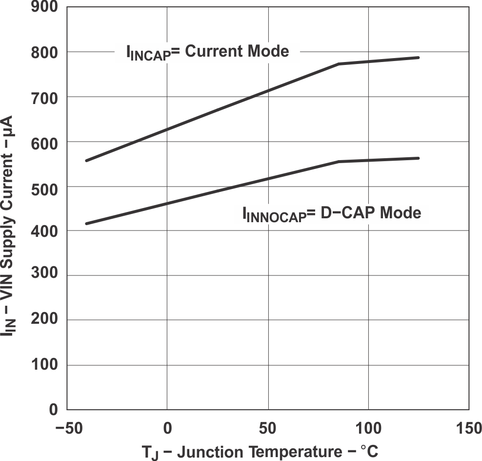 Figure 1. VIN Supply Current vs Junction Temperature
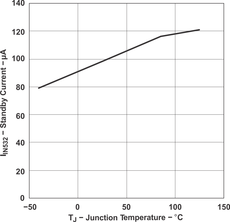 Figure 3. VIN Standby Current vs Junction Temperature
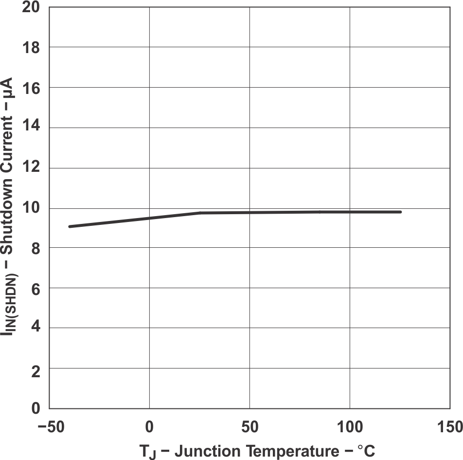 Figure 5. VIN Shutdown Current vs Junction Temperature
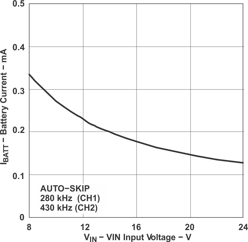 Figure 7. No-Load Battery Current vs Input Voltage
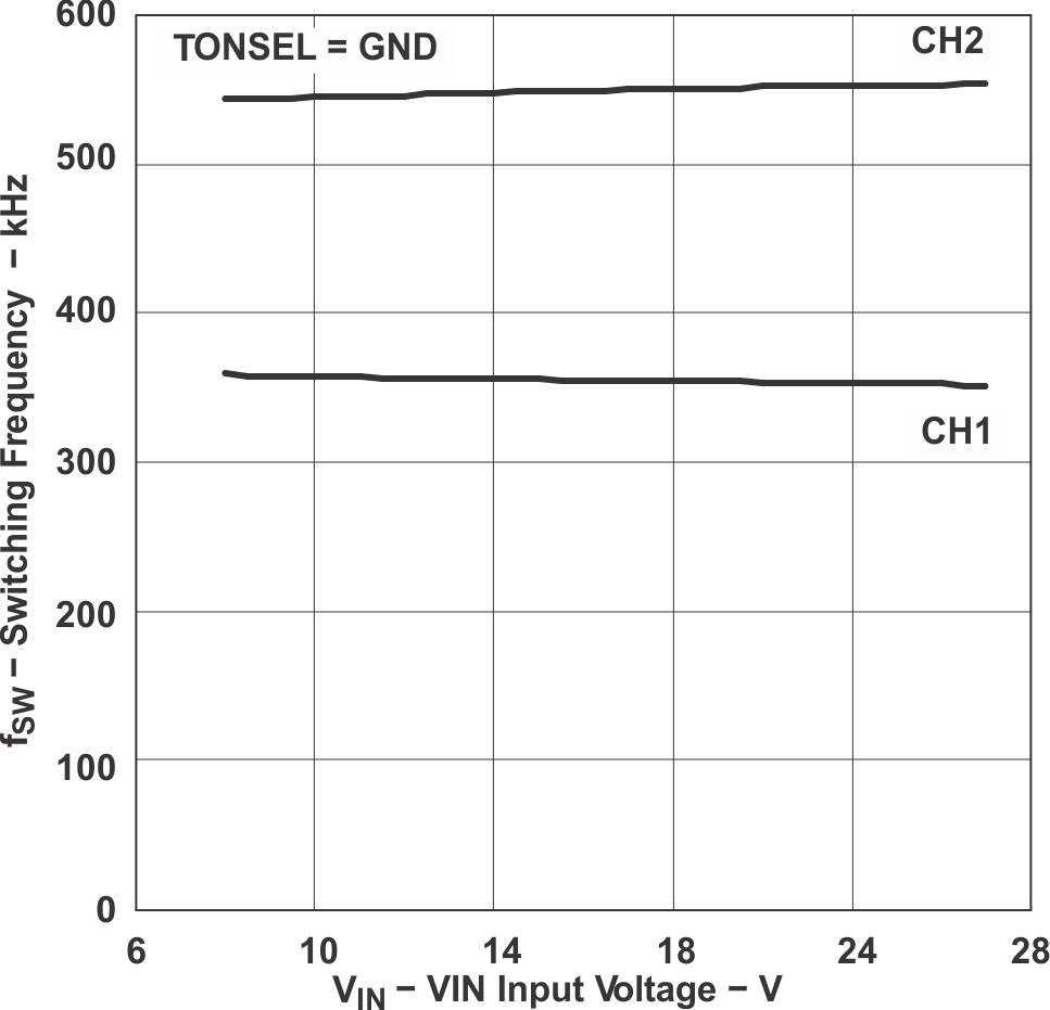 Figure 9. Switching Frequency vs Input Voltage
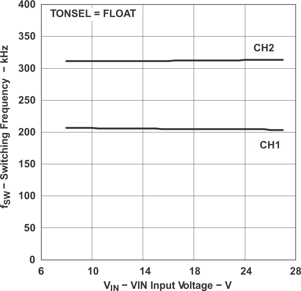 Figure 11. Switching Frequency vs Input Voltage
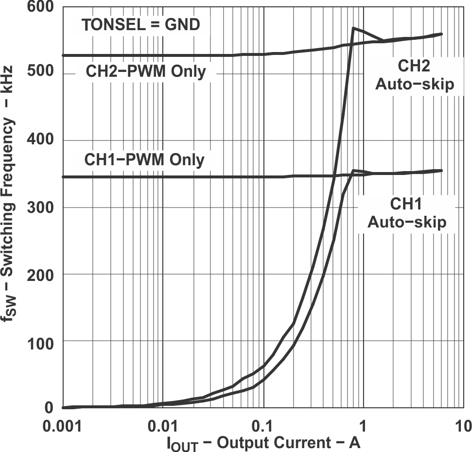 Figure 13. Switching Frequency vs Output Current
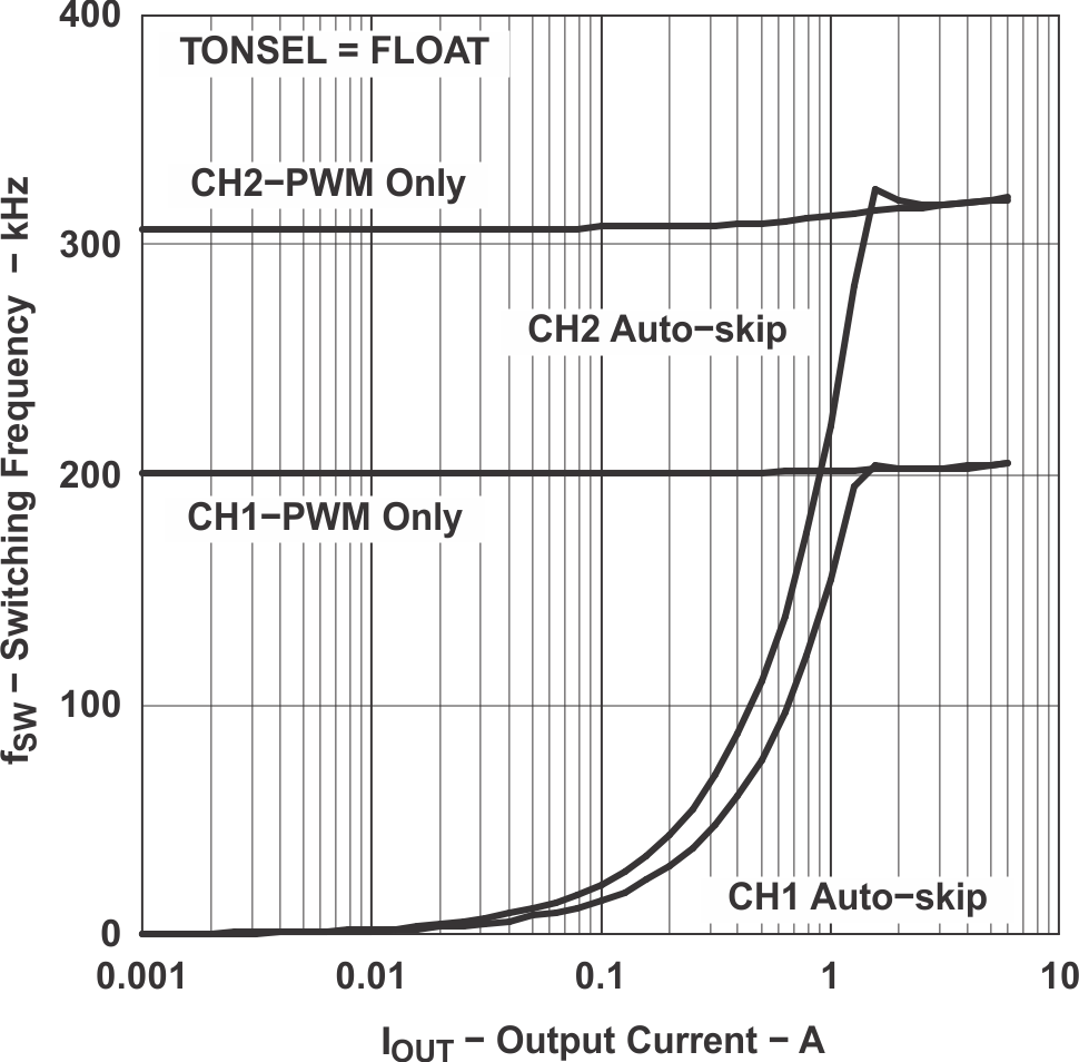 Figure 15. Switching Frequency vs Output Current
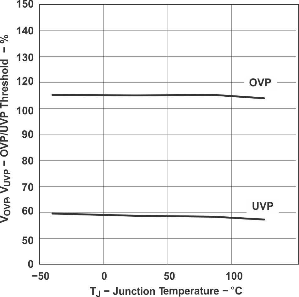 Figure 17. OVP/UVP Threshold Voltage vs Junction Temperature
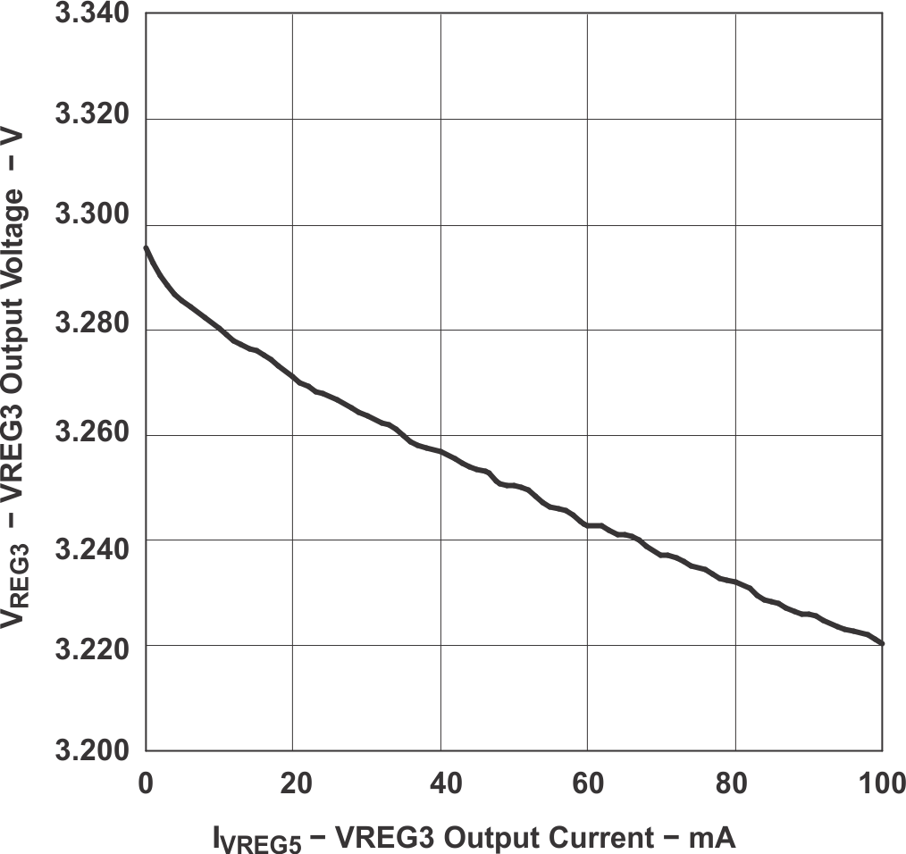 Figure 19. VREG3 Output Voltage vs Output Current
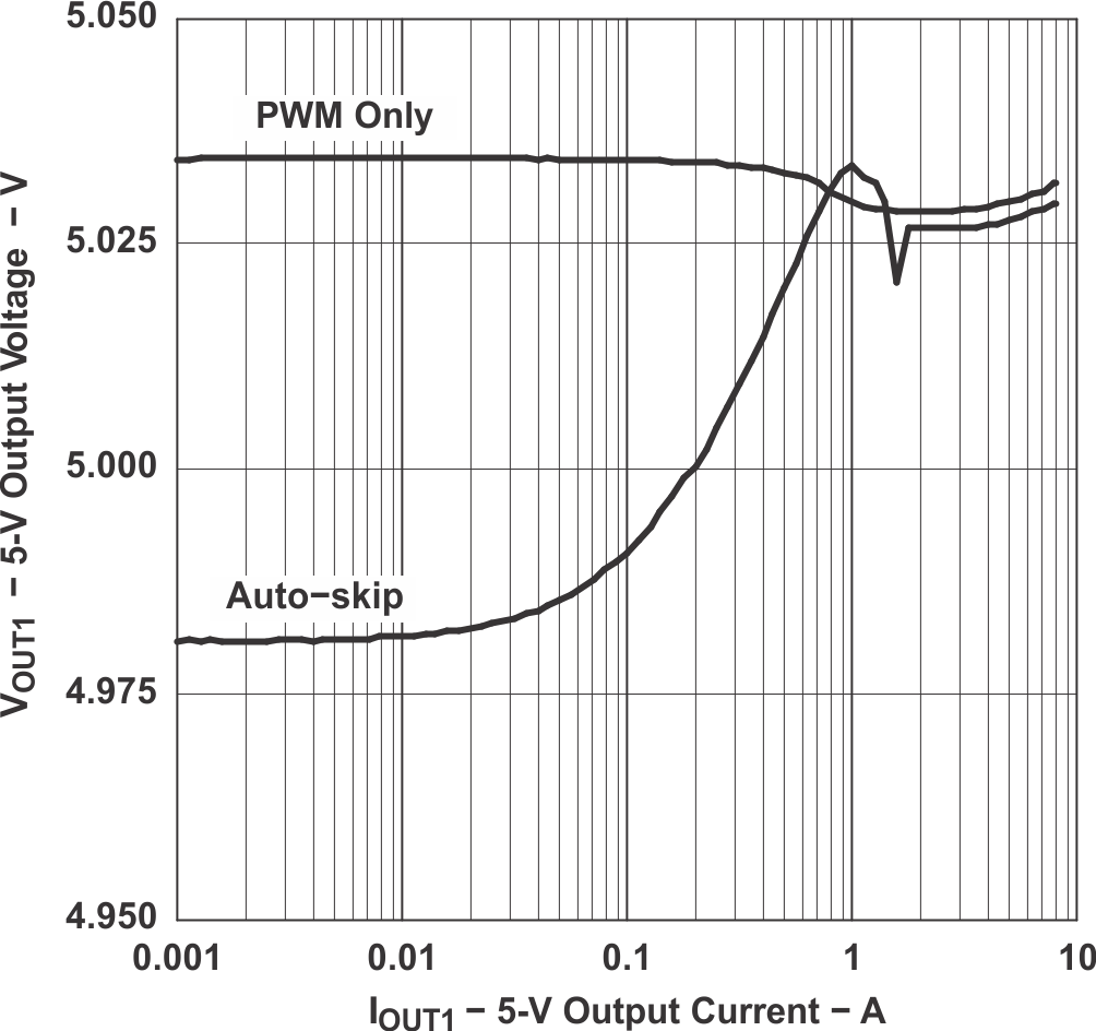 Figure 21. 5-V Output Voltage vs Output Current
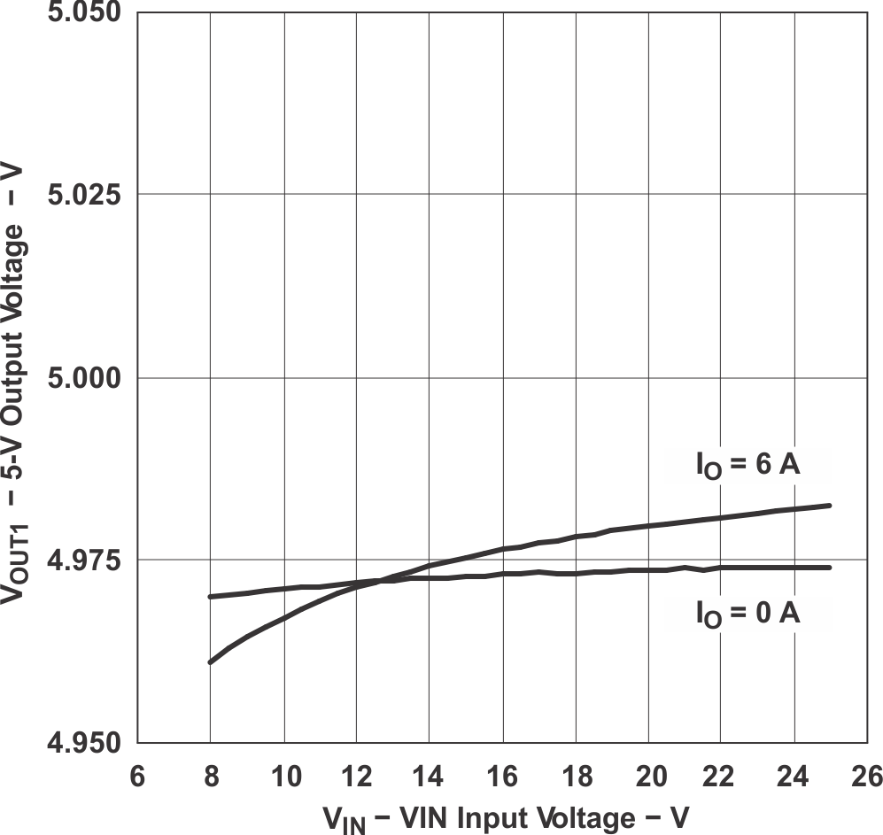 Figure 23. 5-V Output Voltage vs Input Voltage
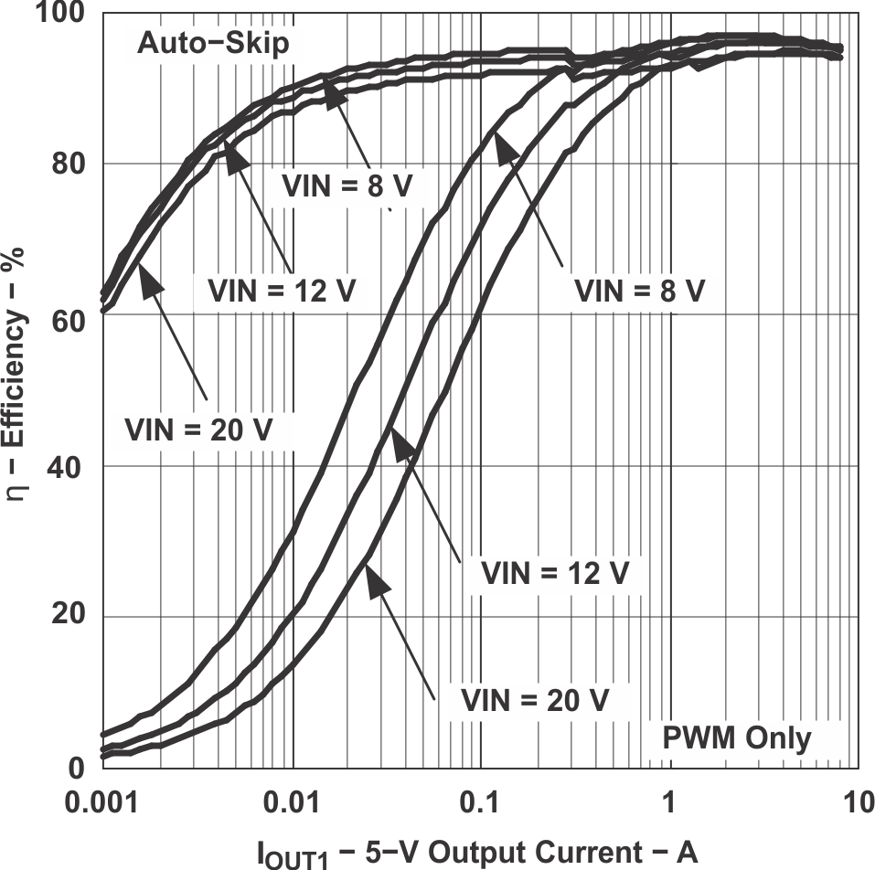 Figure 25. 5-V Efficiency vs Output Current
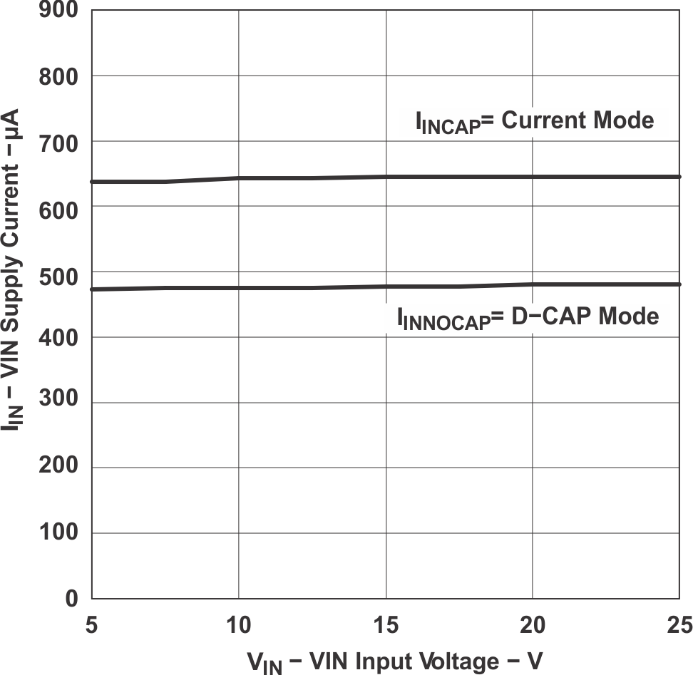 Figure 2. VIN Supply Current vs Input Voltage
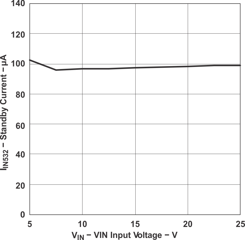 Figure 4. VIN Standby Current vs Input Voltage
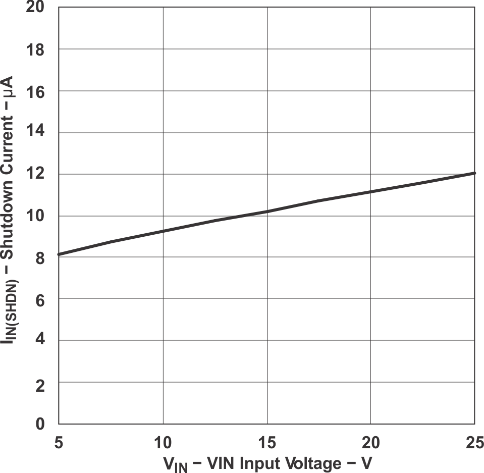 Figure 6. VIN Shutdown Current vs Input Voltage
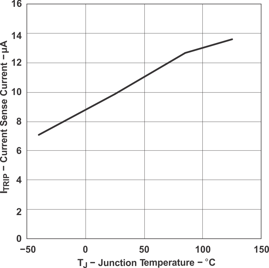 Figure 8. Current Sense Current vs Junction Temperature
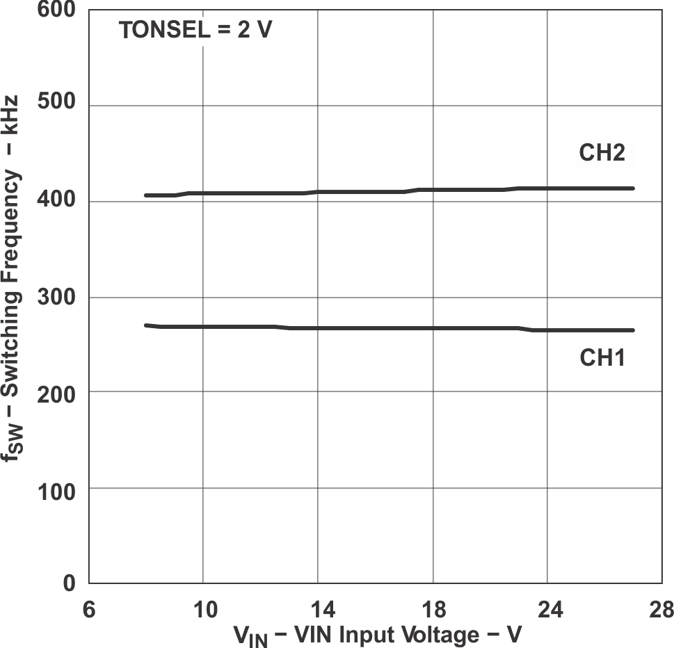 Figure 10. Switching Frequency vs Input Voltage
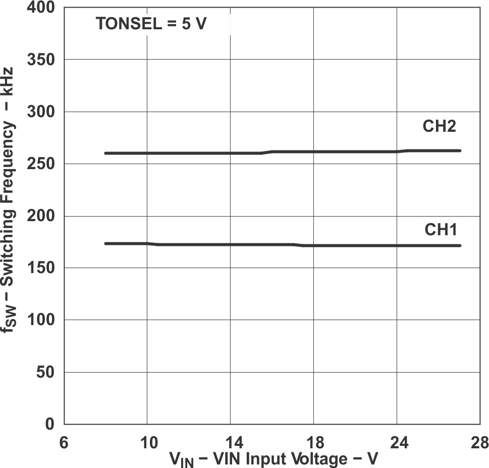 Figure 12. Switching Frequency vs Input Voltage
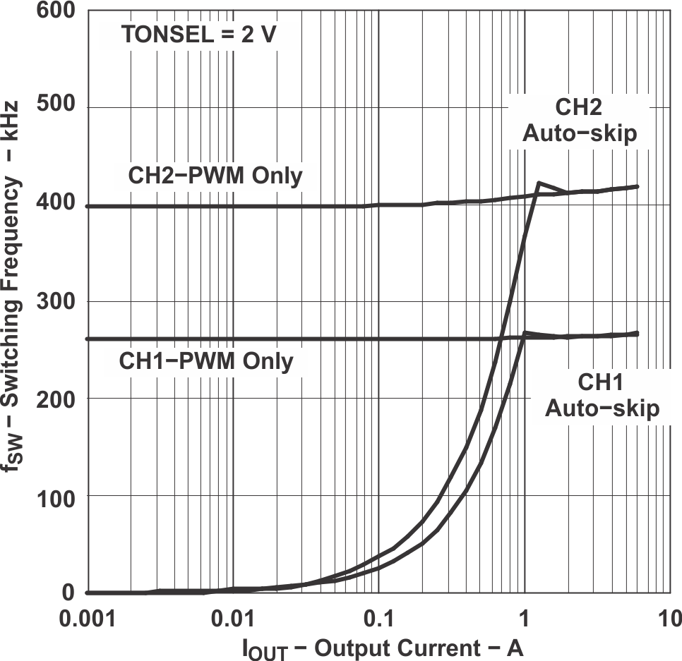 Figure 14. Switching Frequency vs Output Current
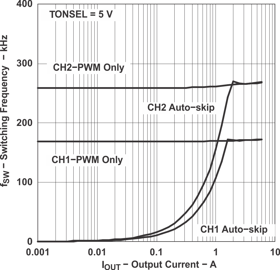 Figure 16. Switching Frequency vs Output Current
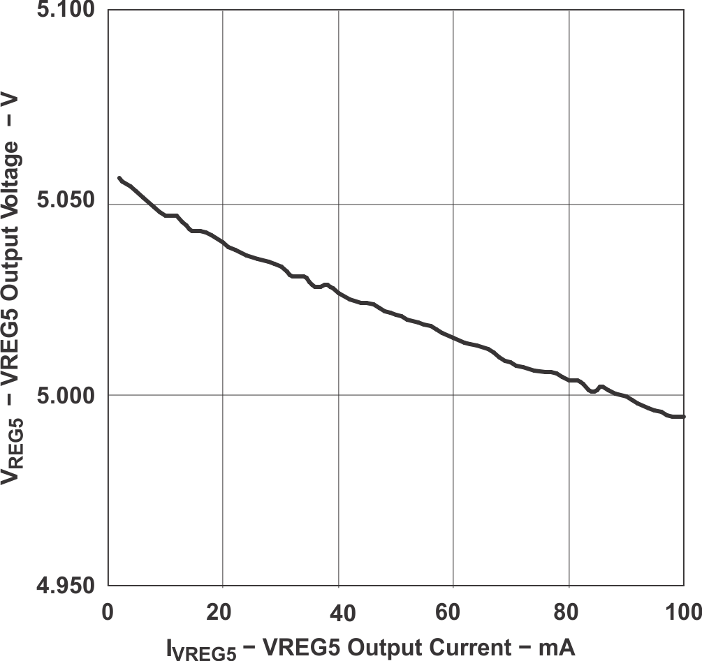 Figure 18. VREG5 Output Voltage vs Output Current
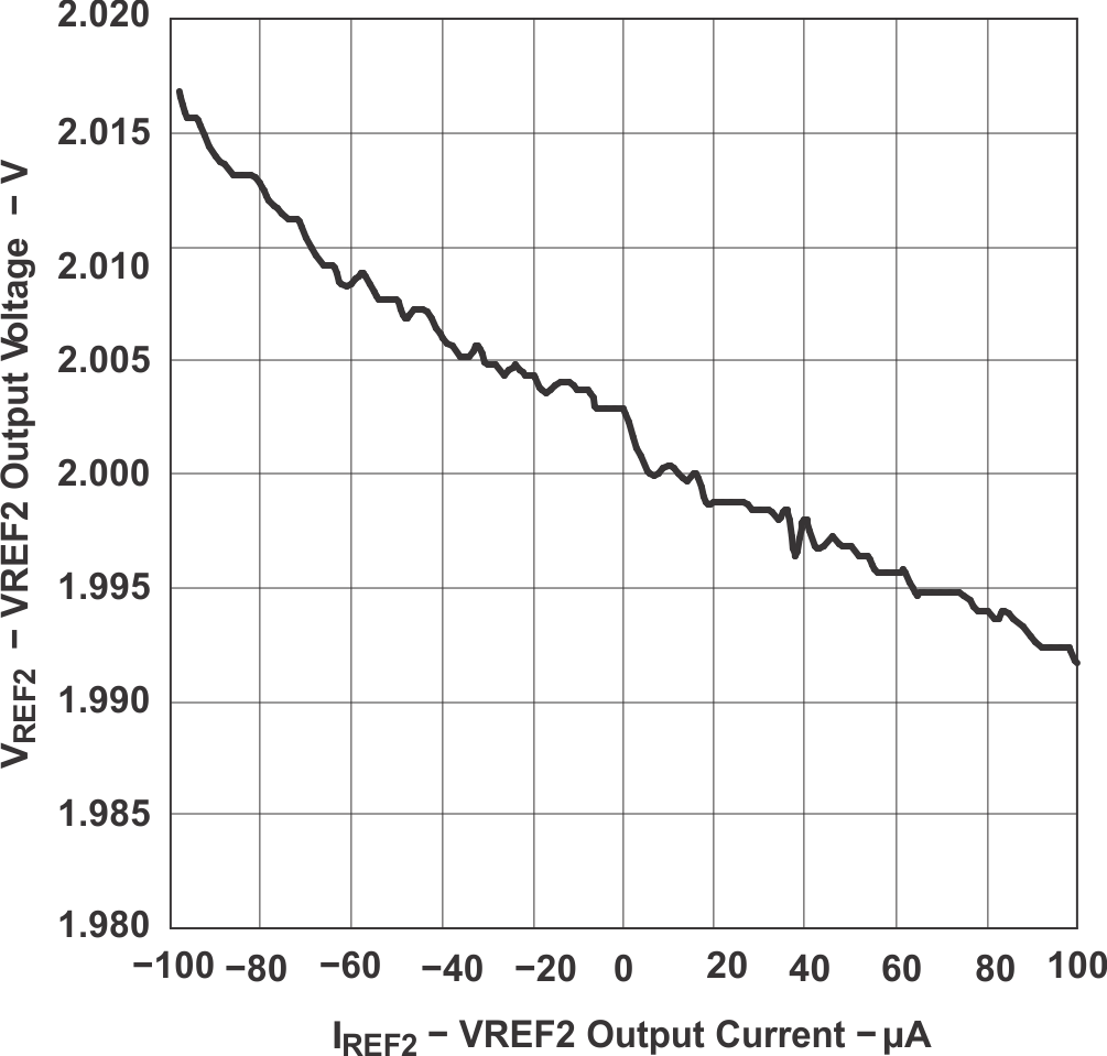 Figure 20. VREF2 Output Voltage vs Output Current
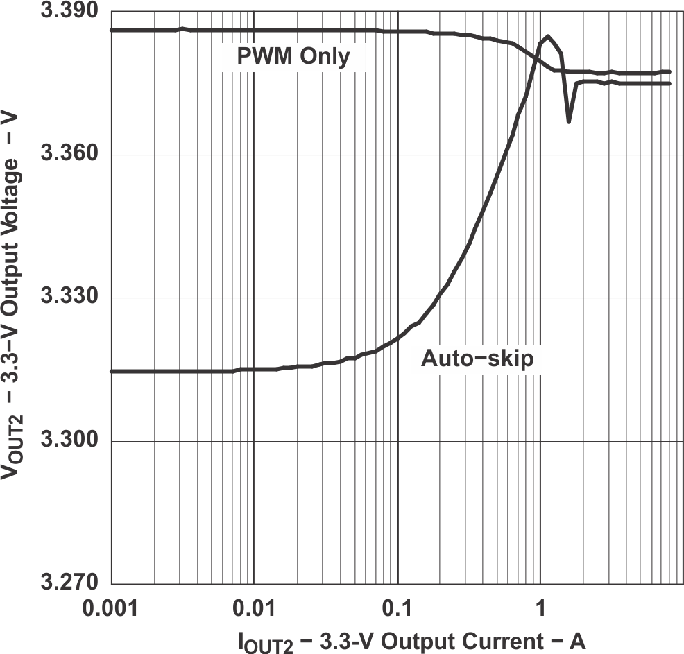 Figure 22. 3.3-V Output Voltage vs Output Current
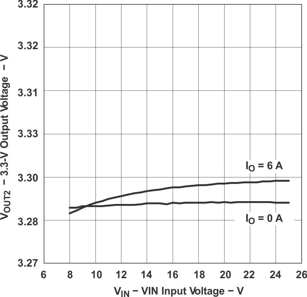 Figure 24. 3.3-V Output Voltage vs Input Voltage
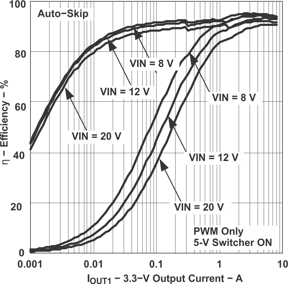 Figure 26. 3.3-V Efficiency vs Output Current