SLVS631C December 2005 – May 2015 TPS51117
PRODUCTION DATA.
- 1 Features
- 2 Applications
- 3 Description
- 4 Revision History
- 5 Pin Configuration and Functions
- 6 Specifications
-
7 Detailed Description
- 7.1 Overview
- 7.2 Functional Block Diagram
- 7.3
Feature Description
- 7.3.1 PWM Frequency and Adaptive On-Time Control
- 7.3.2 Low-Side Driver
- 7.3.3 High-Side Driver
- 7.3.4 Soft-Start
- 7.3.5 Powergood
- 7.3.6 Output Discharge Control (Soft-Stop)
- 7.3.7 Overcurrent Limit
- 7.3.8 Negative Overcurrent Limit (PWM-Only Mode)
- 7.3.9 Overvoltage Protection
- 7.3.10 Undervoltage Protection
- 7.3.11 Start-Up Sequence
- 7.3.12 UVLO Protection
- 7.3.13 Thermal Shutdown
- 7.4 Device Functional Modes
- 8 Application and Implementation
- 9 Power Supply Recommendations
- 10Layout
- 11Device and Documentation Support
- 12Mechanical, Packaging, and Orderable Information
封装选项
请参考 PDF 数据表获取器件具体的封装图。
机械数据 (封装 | 引脚)
- RGY|14
- PW|14
散热焊盘机械数据 (封装 | 引脚)
订购信息
5 Pin Configuration and Functions
RGY Package
14-Pin VQFN
Bottom View
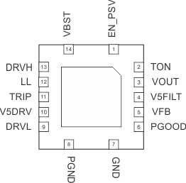
PW Package
14-Pin TSSOP
Top View
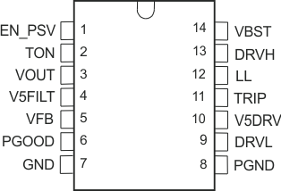
Pin Functions
| PIN | I/O | DESCRIPTION | |
|---|---|---|---|
| NAME | NO. | ||
| DRVH | 13 | O | High-side NFET gate driver output. Source 5 Ω, sink 1.5-Ω LL-node referenced driver. Drive voltage corresponds to VBST to LL voltage. |
| DRVL | 9 | O | Rectifying (low-side) NFET gate driver output. Source 5 Ω, sink 1.5-Ω PGND referenced driver. Drive voltage is V5DRV voltage. |
| EN_PSV | 1 | I | Enable / power save pin. Connect to ground to disable SMPS. Connect to 3.3 V or 5 V to turn on SMPS and activate skip mode. Float to turn on SMPS but disable skip mode (forced continuous conduction mode). |
| GND | 7 | I | Signal ground pin. |
| LL | 12 | I/O | High-side NFET gate driver return. Also serves as anode of overcurrent comparator. |
| PGND | 8 | I/O | Ground return for rectifying NFET gate driver. Also cathode of overcurrent protection and source node of the output discharge switch. |
| PGOOD | 6 | O | Powergood window comparator, open-drain, output. Pull up to 5-V rail with a pullup resistor. Current capability is 7.5 mA. |
| TON | 2 | I | On-time / frequency adjustment pin. Connect to LL with 100-kΩ to 600-kΩ resistor. |
| TRIP | 11 | I | Overcurrent trip point set input. Connect resistor from this pin to signal ground to set threshold for both overcurrent and negative overcurrent limit. |
| VBST | 14 | I | Supply input for high-side NFET gate driver (boost terminal). Connect capacitor from this pin to LL-node. An internal PN diode is connected between V5DRV to this pin. Designer can add external Schottky diode if forward drop is critical to drive the power NFET. |
| VFB | 5 | I | SMPS voltage feedback input. Connect the resistor divider here for adjustable output. |
| VOUT | 3 | I | Connect to SMPS output. This terminal serves two functions: output voltage monitor for on-time adjustment, and input for the output discharge switch. |
| V5DRV | 10 | I | 5-V Power supply input for FET gate drivers. Internally connected to VBST by a PN diode. Connect 1 μF or more between this pin and PGND to support instantaneous current for gate drivers. |
| V5FILT | 4 | I | 5-V Power supply input for all the control circuitry except gate drivers. Supply 5-V ramp rate should be 17 mV/μs or less and Tj < 85°C to secure safe start-up of the internal reference circuit. Apply RC filter consists of 300 Ω + 1 μF or 100 Ω + 4.7 μF at the pin input. |