SLVS631C December 2005 – May 2015 TPS51117
PRODUCTION DATA.
- 1 Features
- 2 Applications
- 3 Description
- 4 Revision History
- 5 Pin Configuration and Functions
- 6 Specifications
-
7 Detailed Description
- 7.1 Overview
- 7.2 Functional Block Diagram
- 7.3
Feature Description
- 7.3.1 PWM Frequency and Adaptive On-Time Control
- 7.3.2 Low-Side Driver
- 7.3.3 High-Side Driver
- 7.3.4 Soft-Start
- 7.3.5 Powergood
- 7.3.6 Output Discharge Control (Soft-Stop)
- 7.3.7 Overcurrent Limit
- 7.3.8 Negative Overcurrent Limit (PWM-Only Mode)
- 7.3.9 Overvoltage Protection
- 7.3.10 Undervoltage Protection
- 7.3.11 Start-Up Sequence
- 7.3.12 UVLO Protection
- 7.3.13 Thermal Shutdown
- 7.4 Device Functional Modes
- 8 Application and Implementation
- 9 Power Supply Recommendations
- 10Layout
- 11Device and Documentation Support
- 12Mechanical, Packaging, and Orderable Information
封装选项
请参考 PDF 数据表获取器件具体的封装图。
机械数据 (封装 | 引脚)
- RGY|14
- PW|14
散热焊盘机械数据 (封装 | 引脚)
订购信息
1 Features
- High Efficiency, Low Power Consumption, 4.5-μA Typical Shutdown Current
- Fixed Frequency Emulated On-Time Control, Adjustable from 100 kHz to 550 kHz
- D-CAP™ Mode With 100-ns Load Step Response
- < 1% Initial Reference Accuracy
- Output Voltage Range: 0.75 V to 5.5 V
- Wide Input Voltage Range: 1.8 V to 28 V
- Selectable Auto-Skip/PWM-Only Operation
- Temperature Compensated (4500 ppm/°C)
Low-Side RDS(on) Overcurrent Sensing - Negative Overcurrent Limit
- Integrated Boost Diode
- Integrated OVP/UVP and Thermal Shutdown
- Powergood Signal
- Internal 1.2-ms Voltage Soft-Start
- Integrated Output Discharge (Soft-Stop)
2 Applications
- Notebook Computers
- I/O Supplies
- System Power Supplies
3 Description
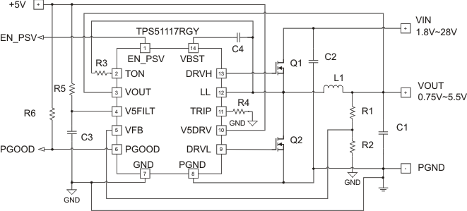
The TPS51117 device is a cost-effective, synchronous buck controller for POL voltage regulation in notebook PC applications. The controller is dedicated for the operation of the Adaptive On-Time D-CAP mode. This mode provides ease-of-use, low external component count, and fast transient response. Auto-skip mode for high efficiency down to the milliampere load range, or PWM-only mode for low-noise operation is selectable.
The current-sensing scheme for positive overcurrent and negative overcurrent protection is loss-less low-side RDS(on) sensing plus temperature compensation. The device receives a 5-V (4.5 V to
5.5 V) supply from another regulator such as the TPS51120 or TPS51020. The conversion input can be either VBAT or a 5-V rail, ranging from 1.8 V to
28 V, and the output voltage range is from 0.75 V to 5.5 V.
The TPS51117 is available in a 14-pin VQFN or a 14-pin TSSOP package and is specified from –40°C to 85°C.
Device Information(1)
| PART NUMBER | PACKAGE | BODY SIZE (NOM) |
|---|---|---|
| TPS51117 | TSSOP (14) | 4.40 mm × 5.00 mm |
| VQFN (14) | 3.50 mm × 3.50 mm |
- For all available packages, see the orderable addendum at the end of the data sheet.
Typical Application Circuit