SLVSAR7E June 2011 – October 2016 TPS43350-Q1 , TPS43351-Q1
PRODUCTION DATA.
- 1 Features
- 2 Applications
- 3 Description
- 4 Revision History
- 5 Pin Configuration and Functions
- 6 Specifications
-
7 Detailed Description
- 7.1 Overview
- 7.2 Functional Block Diagram
- 7.3
Feature Description
- 7.3.1
Buck Controllers: Normal Mode PWM Operation
- 7.3.1.1 Frequency Selection and External Synchronization
- 7.3.1.2 Enable Inputs
- 7.3.1.3 Feedback Inputs
- 7.3.1.4 Soft-Start Inputs
- 7.3.1.5 Current-Mode Operation
- 7.3.1.6 Current Sensing and Current Limit With Foldback
- 7.3.1.7 Slope Compensation
- 7.3.1.8 Power-Good Outputs and Filter Delays
- 7.3.1.9 Light-Load PFM Mode
- 7.3.2 Frequency-Hopping Spread Spectrum (TPS43351-Q1 Only)
- 7.3.3 Gate-Driver Supply (VREG, EXTSUP)
- 7.3.4 External P-Channel Drive (GC2) and Reverse-Battery Protection
- 7.3.5 Undervoltage Lockout and Overvoltage Protection
- 7.3.6 Thermal Protection
- 7.3.1
Buck Controllers: Normal Mode PWM Operation
- 7.4 Device Functional Modes
-
8 Application and Implementation
- 8.1 Application Information
- 8.2
Typical Application
- 8.2.1 Design Requirements
- 8.2.2
Detailed Design Procedure
- 8.2.2.1 BuckA Component Selection
- 8.2.2.2 Inductor Selection L
- 8.2.2.3 Inductor Ripple Current IRIPPLE
- 8.2.2.4 Output Capacitor COUTA
- 8.2.2.5 Bandwidth of Buck Converter fC
- 8.2.2.6 Selection of Components for Type II Compensation
- 8.2.2.7 Resistor Divider Selection for Setting VOUTA Voltage
- 8.2.2.8 BuckB Component Selection
- 8.2.2.9 Resistor Divider Selection for Setting VOUT Voltage
- 8.2.2.10 BUCKx High-Side and Low-Side N-Channel MOSFETs
- 8.2.3 Application Curves
- 9 Power Supply Recommendations
- 10Layout
- 11Device and Documentation Support
- 12Mechanical, Packaging, and Orderable Information
6 Specifications
6.1 Absolute Maximum Ratings
over operating free-air temperature range (unless otherwise noted)(1)
(1) Stresses beyond those listed under Absolute Maximum Ratings may cause permanent damage to the device. These are stress ratings only, which do not imply functional operation of the device at these or any other conditions beyond those indicated under Recommended Operating Conditions. Exposure to absolute-maximum-rated conditions for extended periods may affect device reliability. All voltage values are with respect to AGND, unless otherwise stated.
6.2 ESD Ratings
| VALUE | UNIT | ||||
|---|---|---|---|---|---|
| V(ESD) | Electrostatic discharge | Human-body model (HBM) AEC-Q100 Classification Level H2(1) | ±2000 | V | |
| Charged-device model (CDM) AEC-Q100 Classification Level C2 | Pins 12, 21, 22, and 27 | ±400 | |||
| Pins 1 and 20 | ±750 | ||||
| All other pins | ±500 | ||||
| Machine model (MM) | Pins 15 and 24 | ±150 | |||
| All other pins | ±200 | ||||
(1) AEC Q100-002 indicates that HBM stressing shall be in accordance with the ANSI/ESDA/JEDEC JS-001 specification.
6.3 Recommended Operating Conditions
over operating free-air temperature range (unless otherwise noted)| MIN | MAX | UNIT | ||
|---|---|---|---|---|
| Buck function: BuckA and BuckB voltage |
Input voltage: , VBAT | 4 | 40 | V |
| Enable inputs: ENA, ENB | 0 | 40 | V | |
| Boot inputs: CBA, CBB | 4 | 48 | V | |
| Phase inputs: PHA, PHB | –0.6 | 40 | V | |
| Current-sense voltage: SA1, SA2, SB1, SB2 | 0 | 11 | V | |
| Power-good output: PGA, PGB | 0 | 11 | V | |
| SYNC, EXTSUP | 0 | 9 | V | |
| Temperature | Operating temperature: TA | –40 | 125 | °C |
6.4 Thermal Information
| THERMAL METRIC(1) | TPS43333-Q1 | UNIT | |
|---|---|---|---|
| DAP (HTSSOP) | |||
| 38 PINS | |||
| RθJA | Junction-to-ambient thermal resistance | 27.3 | °C/W |
| RθJC(top) | Junction-to-case (top) thermal resistance | 19.6 | °C/W |
| RθJB | Junction-to-board thermal resistance | 15.9 | °C/W |
| ψJT | Junction-to-top characterization parameter | 0.24 | °C/W |
| ψJB | Junction-to-board characterization parameter | 6.6 | °C/W |
| RθJC(bot) | Junction-to-case (bottom) thermal resistance | 1.2 | °C/W |
(1) For more information about traditional and new thermal metrics, see the Semiconductor and IC Package Thermal Metrics application report.
6.5 DC Electrical Characteristics
VIN = 8 V to 18 V, TJ = –40°C to 150°C (unless otherwise noted)| NO. | PARAMETER | TEST CONDITIONS | MIN | TYP | MAX | UNIT | |
|---|---|---|---|---|---|---|---|
| 1.0 | Input Supply | ||||||
| 1.1 | VBat | Supply voltage | After initial start-up, condition is satisfied. | 4 | 40 | V | |
| 1.2 | VIN | Input voltage required for device on initial start-up | 6.5 | 40 | V | ||
| Buck regulator operating range after initial start-up | 4 | 40 | V | ||||
| 1.3 | VIN UV | Buck undervoltage lockout | VIN falling. After a reset, initial start-up conditions may apply.(1) | 3.5 | 3.6 | 3.8 | V |
| VIN rising. After a reset, initial start-up conditions may apply.(1) | 3.8 | 4 | V | ||||
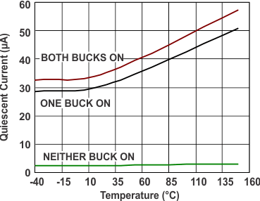
| 1.5 | Iq_LPM_ | LPM quiescent current: TA = 25°C(2) |
VIN = 13 V, BuckA: LPM, BuckB: off | 30 | 40 | µA | |
| VIN = 13 V, BuckB: LPM, BuckA: off | 30 | 40 | |||||
| VIN = 13 V, BuckA, B: LPM | 35 | 45 | µA | ||||
| 1.6 | Iq_LPM | LPM quiescent current: TA = 125°C(2) |
VIN = 13 V, BuckA: LPM, BuckB: off | 40 | 50 | µA | |
| VIN = 13 V, BuckB: LPM, BuckA: off | 40 | 50 | |||||
| VIN = 13 V, BuckA, B: LPM | 45 | 55 | µA | ||||
| 1.7 | Iq_NRM | Quiescent current: TA = 25°C(2) |
Normal operation, SYNC = High | 4.85 | 5.3 | mA | |
| VIN = 13 V, BuckA: CCM, BuckB: off | 7 | 7.6 | mA | ||||
| VIN = 13 V, BuckB: CCM, BuckA: off | |||||||
| VIN = 13 V, BuckA, B: CCM | |||||||
| 1.8 | Iq_NRM | Quiescent current: TA = 125°C(2) |
Normal operation, SYNC = High | 5 | 5.5 | mA | |
| VIN = 13 V, BuckA: CCM, BuckB: off | 7.5 | 8 | mA | ||||
| VIN = 13 V, BuckB: CCM, BuckA: off | |||||||
| VIN = 13 V, BuckA, B: CCM | |||||||
| 1.9 | IBAT_sh | Shutdown current | BuckA, B: off, VBAT = 13 V | 3 | 5 | µA | |
| 2.0 | Input Voltage - Overvoltage Lockout | ||||||
| 2.1 | VOVLO | Overvoltage shutdown | VIN rising | 45 | 46 | 47 | V |
| VIN falling | 43 | 44 | 45 | V | |||
| 2.2 | OVLOHys | Hysteresis | 1 | 2 | 3 | V | |
| 2.3 | OVLOfilter | Filter time | 5 | µs | |||
| Gate Driver for PMOS | |||||||
| 3.1 | rDS(on) | PMOS OFF | 10 | 20 | Ω | ||
| 3.2 | IPMOS_ON | Gate current | VIN = 13.5 V, VGS = –5 V | 10 | mA | ||
| 3.3 | tdelay_ON | Turnon delay | C = 10 nF | 5 | 10 | µs | |
| 4.0 | Buck Controllers | ||||||
| 4.1 | VBuckA/B | Adjustable output voltage range | 0.9 | 11 | V | ||
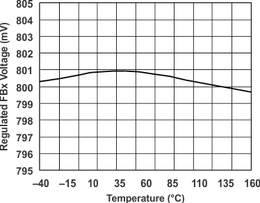
| 4.2 | VREF, NRM | Internal reference voltage and tolerance in normal mode | Measure FBX pin | 0.792 | 0.8 | 0.808 | V |
| –1% | 1% | ||||||
| 4.3 | VREF, LPM | Internal reference voltage and tolerance in low-power mode | Measure FBX pin | 0.784 | 0.8 | 0.816 | V |
| –2% | 2% | ||||||
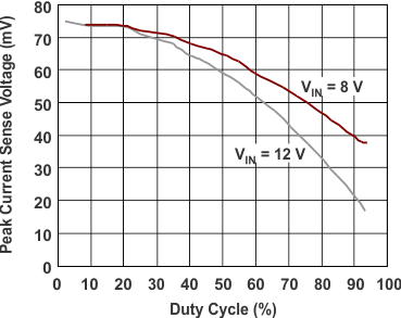
| 4.4 | VSENSE | V sense for forward current limit in CCM | FBx = 0.75 V (low duty cycles) | 60 | 75 | 90 | mV |
| 4.5 | V sense for reverse current limit in CCM | FBx = 1 V | –65 | –37.5 | –23 | mV | |
| 4.6 | VI-Foldback | V sense for output short | FBx = 0 V | 17 | 32.5 | 48 | mV |
| 4.7 | tdead | Shoot-through delay, blanking time | 100 | ns | |||
| 4.8 | DCNRM | High-side minimum on-time | 100 | ns | |||
| Maximum duty cycle (digitally controlled) | 98.75% | ||||||
| 4.9 | DCLPM | Duty cycle LPM | 80% | ||||
| 4.10 | ILPM_Entry | LPM entry threshold load current as fraction of maximum set load current | The exit threshold is specified to be always higher than entry threshold | 1% | . See(3) | ||
| ILPM_Exit | LPM exit threshold load current as fraction of maximum set load current | The exit threshold is specified to be always higher than entry threshold | See(3) | 10% | |||
| High-Side External NMOS Gate Drivers for Buck Controller | |||||||
| 4.11 | IGX1_peak | Gate driver peak current | 1.5 | A | |||
| 4.12 | rDS(on) | Source and sink driver | VREG = 5.8 V, IGX1 current = 200 mA | 2 | Ω | ||
| Low-Side NMOS Gate Drivers for Buck Controller | |||||||
| 4.13 | IGX2_peak | Gate-driver peak current | 1.5 | A | |||
| 4.14 | rDS(on) | Source and sink driver | VREG = 5.8 V, IGX2 current = 200 mA | 2 | Ω | ||
| Error Amplifier (OTA) for Buck Converters | |||||||
| 4.15 | GmBUCK | Transconductance | COMPA, COMPB = 0.8 V, source/sink = 5 µA, test in feedback loop |
0.72 | 1 | 1.35 | mS |
| 4.16 | IPULLUP_FBx | Pullup current at FBx pins | FBx = 0 V | 50 | 100 | 200 | nA |
| 5.0 | Digital Inputs: ENA, ENB, SYNC | ||||||
| 5.1 | VIH | Higher threshold | VIN = 13 V | 1.7 | V | ||
| 5.2 | VIL | Lower threshold | VIN = 13 V | 0.7 | V | ||
| 5.3 | RIH_SYNC | Resistance | VSYNC = 5 V | 500 | kΩ | ||
| 5.5 | IIL_ENx | Pullup current source on ENA, ENB | VENx = 0 V | 0.5 | 2 | µA | |
| 6.0 | Switching Parameters – Buck DC-DC Controllers | ||||||
| 6.1 | fSW_Buck | Buck switching frequency | RT pin: GND | 360 | 400 | 440 | kHz |
| 6.2 | fSW_Buck | Buck switching frequency | RT pin: 60-kΩ external resistor | 360 | 400 | 440 | kHz |
| 6.3 | fSW_adj | Buck adjustable range with external resistor | RT pin: external resistor | 150 | 600 | kHz | |
| 6.4 | fSYNC | Buck synchronization range | External clock input | 150 | 600 | kHz | |
| 6.5 | fSS | Spread-spectrum spreading | TPS43351-Q1 only | 5% | |||
| 7.0 | Internal Gate-Driver Supply | ||||||
| 7.1 | VREG | Internal regulated supply | VIN = 8 V to 18 V, EXTSUP = 0 V, SYNC = High | 5.5 | 5.8 | 6.1 | V |
| Load regulation | IVREG = 0 mA to 100 mA, EXTSUP = 0 V, SYNC = High |
0.2% | 1% | ||||
| 7.2 | VREG(EXTSUP) | Internal regulated supply | EXTSUP = 8.5 V | 7.2 | 7.5 | 7.8 | V |
| Load regulation | IEXTSUP = 0 mA to 125 mA, SYNC = High EXTSUP = 8.5 V to 13 V |
0.2% | 1% | ||||
| 7.3 | VEXTSUP_th | EXTSUP switch-over voltage threshold | IVREG = 0 mA to 100 mA , EXTSUP ramping positive |
4.4 | 4.6 | 4.8 | V |
| 7.4 | VEXTSUP-Hys | EXTSUP switch-over hysteresis | 150 | 250 | mV | ||
| 7.5 | IREG-Limit | Current limit on VREG | EXTSUP = 0 V, normal mode as well as LPM | 100 | 400 | mA | |
| 7.6 | IREG_EXTSUP-Limit | Current limit on VREG when using EXTSUP | IVREG = 0 mA to 100 mA, EXTSUP = 8.5 V, SYNC = High |
125 | 400 | mA | |
| 8.0 | Soft Start | ||||||
| 8.1 | ISSx | Soft-start source current | SSA and SSB = 0 V | 0.75 | 1 | 1.25 | µA |
| 9.0 | Oscillator (RT) | ||||||
| 9.1 | VRT | Oscillator reference voltage | 1.2 | V | |||
| 10.0 | Power-Good / Delay | ||||||
| 10.1 | PGpullup | Pullup for A and B to Sx2 | 50 | kΩ | |||
| 10.2 | PGth1 | Power-good threshold | FBx falling | –5% | –7% | –9% | |
| 10.3 | PGhys | Hysteresis | 2% | ||||
| 10.4 | PGdrop | Voltage drop | IPGA = 5 mA | 450 | mV | ||
| 10.5 | IPGA = 1 mA | 100 | mV | ||||
| 10.6 | PGleak | Leakage | VSx2 = VPGx = 13 V | 1 | µA | ||
| 10.7 | tdeglitch | Power-good deglitch time | 2 | 16 | µs | ||
| 10.8 | tdelay | Reset delay | External capacitor = 1 nF VBuckX < PGth1 |
1 | ms | ||
| 10.9 | tdelay_fix | Fixed reset delay | No external capacitor, pin open | 20 | 50 | µs | |
| 10.10 | IOH | Activate current source (current to charge external capacitor) | 30 | 40 | 50 | µA | |
| 10.11 | IIL | Activate current sink (current to discharge external capacitor) | 30 | 40 | 50 | µA | |
| 11.0 | Overtemperature Protection | ||||||
| 11.1 | Tshutdown | Junction temperature shutdown threshold | 150 | 165 | °C | ||
| 11.2 | Thys | Junction temperature hysteresis | 15 | °C | |||
(1) If VBAT and VREG remain adequate, the buck can continue to operate if VIN is > 3.8 V.
(2) Quiescent current specification is non-switching current consumption without including the current in the external feedback resistor divider.
(3) The exit threshold specification is to be always higher than the entry threshold.
6.6 Power Dissipation Derating Profile, 38-Pin HTTSOP PowerPAD Package
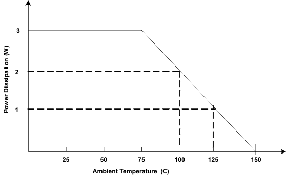 Figure 1. Power Dissipation Derating Profile Based on High-K JEDEC PCB
6.7 Typical Characteristics
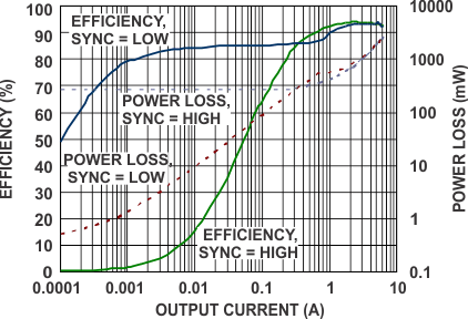
| VIN = 12 V | VOUT = 5 V | fSW = 400 kHz |
| L = 4.7 µH | RSENSE = 10 mΩ |
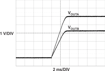
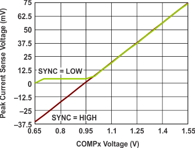
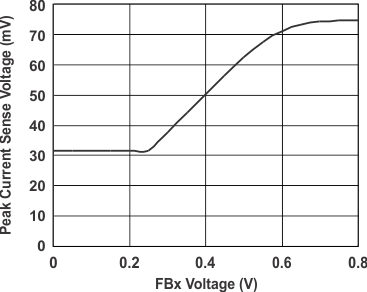
| VIN = 12 V | VOUT = 5 V | fSW = 400 kHz |
| L = 4.7 µH | RSENSE = 10 mΩ |
