SLUS660I September 2005 – January 2015 TPS40140
PRODUCTION DATA.
- 1 Features
- 2 Applications
- 3 Description
- 4 Revision History
- 5 Device Comparison Table
- 6 Pin Configuration and Functions
- 7 Specifications
- 8 Detailed Description
-
9 Application and Implementation
- 9.1
Application Information
- 9.1.1 Synchronizing a Single Controller to an External Clock
- 9.1.2 Split Input Voltage Operation
- 9.1.3 Configuring Single and Multiple ICs
- 9.1.4 Digital Clock Synchronization
- 9.1.5 Typical Start-Up Sequence
- 9.1.6 Track (Soft-Start Without PreBiased Output)
- 9.1.7 Soft-Start With PreBiased Outputs
- 9.1.8 Track Function in Configuring a Slave Channel
- 9.1.9 Differential Amplifier, U9
- 9.1.10 Setting the Output Voltage
- 9.1.11 Programmable Input UVLO Protection
- 9.1.12 CLKFLT, CLKIO Pin Fault
- 9.1.13 PHSEL Pin Fault
- 9.1.14 Overtemperature
- 9.1.15 Fault Masking Operation
- 9.1.16 Setting the Switching Frequency
- 9.1.17 Current Sense
- 9.1.18 Current Sensing and Balancing
- 9.1.19 Overcurrent Detection and Hiccup Mode
- 9.1.20 Calculating Overcurrent Protection Level
- 9.1.21 Design Examples Information
- 9.2
Typical Application
- 9.2.1
Application 1: Dual-Output Configuration from 12 to 3.3 V and 1.5 V DC-DC Converter Using a TPS40140
- 9.2.1.1 Design Requirements
- 9.2.1.2
Detailed Design Procedure
- 9.2.1.2.1 Step 1: Inductor Selection
- 9.2.1.2.2 Step 2: Output Capacitor Selection
- 9.2.1.2.3 Step 3: Input Capacitor Selection
- 9.2.1.2.4 Step 4: MOSFET Selection
- 9.2.1.2.5
Step 5: Peripheral Component Design
- 9.2.1.2.5.1 Switching Frequency Setting (RT Pin 5)
- 9.2.1.2.5.2 Output Voltage Setting (FB1 Pin 36)
- 9.2.1.2.5.3 Current Sensing Network Design (CS1 Pin 31 and CSRT1 Pin 32)
- 9.2.1.2.5.4 Overcurrent Protection (ILIM1 Pin 34)
- 9.2.1.2.5.5 VREG (Pin 21)
- 9.2.1.2.5.6 BP5 (Pin 8)
- 9.2.1.2.5.7 PHSEL (Pin 4)
- 9.2.1.2.5.8 VSHARE (Pin 6)
- 9.2.1.2.5.9 PGOOD1 (Pin 30)
- 9.2.1.2.5.10 UVLO_CE1 (Pin 29)
- 9.2.1.2.5.11 Clkio (Pin 28)
- 9.2.1.2.5.12 BOOT1 and SW1 (Pin 27 and 25)
- 9.2.1.2.5.13 TRK1 (Pin 33)
- 9.2.1.2.5.14 DIFFO, VOUT, and GSNS (Pin 1, Pin 2, and Pin 3)
- 9.2.1.2.6 Feedback Compensator Design (COMP1 Pin 35)
- 9.2.1.3 Application Curves
- 9.2.2
Application 2: Two-Phase Single Output Configuration from 12 to 1.5 V DC-DC Converter Using a TPS40140
- 9.2.2.1 Design Requirements
- 9.2.2.2
Detailed Design Procedure
- 9.2.2.2.1 Step 1: Output Capacitor Selection
- 9.2.2.2.2 Step 2: Input Capacitor Selection
- 9.2.2.2.3
Step 3: Peripheral Component Design
- 9.2.2.2.3.1 Switching Frequency Setting (Rt Pin 5)
- 9.2.2.2.3.2 COMP1 and COMP2 (Pin 35 and Pin 10)
- 9.2.2.2.3.3 TRK1 and TRK2 (Pin 33 and Pin 12)
- 9.2.2.2.3.4 ILIM1 and ILIM2 (Pin 34 and Pin 11)
- 9.2.2.2.3.5 FB1 and FB2 (Pin 36 and Pin 9)
- 9.2.2.2.3.6 PHSEL (Pin 4)
- 9.2.2.2.3.7 PGOOD1 and PGOOD2 (Pin 30 and Pin 15)
- 9.2.2.2.3.8 CLKIO (Pin 28)
- 9.2.2.2.3.9 DIFFO, VOUT, and GSNS (Pin 1, Pin 2, and Pin 3)
- 9.2.3 Application Curves
- 9.2.1
Application 1: Dual-Output Configuration from 12 to 3.3 V and 1.5 V DC-DC Converter Using a TPS40140
- 9.3
System Example
- 9.3.1
Four-Phase Single Output Configuration from 12 to 1.8 V DC-DC Converter Using Two TPS40140
- 9.3.1.1 Step 1: Output Capacitor Selection
- 9.3.1.2 Step 2: Input Capacitor Selection
- 9.3.1.3
Step 3: Peripheral Component Design
- 9.3.1.3.1
Master Module
- 9.3.1.3.1.1 Rt (Pin 5)
- 9.3.1.3.1.2 COMP1 and COMP2 (Pin 35 and Pin 10)
- 9.3.1.3.1.3 TRK1 and TRK2 (Pin 33 and Pin 12)
- 9.3.1.3.1.4 ILIM1 and ILIM2 (Pin 34 and Pin 11)
- 9.3.1.3.1.5 FB1 and FB2 (Pin 36 and Pin 9)
- 9.3.1.3.1.6 PHSEL (Pin 4)
- 9.3.1.3.1.7 PGOOD1 and PGOOD2 (Pin 30 and Pin 15)
- 9.3.1.3.1.8 CLKIO (Pin 28)
- 9.3.1.3.2
Slave Module:
- 9.3.1.3.2.1 RT (Pin 5)
- 9.3.1.3.2.2 COMP1 and COMP2 (Pin 35 and Pin 10)
- 9.3.1.3.2.3 TRK1 and TRK2 (Pin 33 and Pin 12)
- 9.3.1.3.2.4 ILIM1 and ILIM2 ( Pin 34 and Pin 11)
- 9.3.1.3.2.5 FB1 and FB2 (Pin 36 and Pin 9)
- 9.3.1.3.2.6 PHSEL (Pin 4)
- 9.3.1.3.2.7 PGOOD1 and PGOOD2 (Pin 30 and Pin 15)
- 9.3.1.3.2.8 CLKIO (Pin 28)
- 9.3.1.3.1
Master Module
- 9.3.1
Four-Phase Single Output Configuration from 12 to 1.8 V DC-DC Converter Using Two TPS40140
- 9.1
Application Information
- 10Power Supply Recommendations
- 11Layout
- 12Device and Documentation Support
- 13Mechanical, Packaging, and Orderable Information
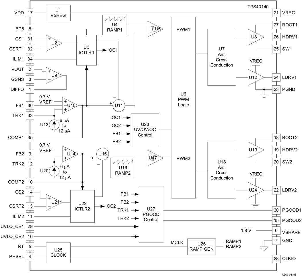
8 Detailed Description
8.1 Overview
The TPS40140 operates with a programmable fixed switching frequency. It is a current feedback controller with forced phase current balancing. When compared to voltage mode control, the current feedback controller results in a simplified feedback network and reduced input line sensitivity. Phase current is sensed by using either the direct current resistance (DCR) of the filter inductors or current sense resistors installed in series with the output. See the section Inductor DCR Current Sense. The current signal is then amplified and superimposed on the amplified voltage error signal to provide current mode PWM control.
Other features include programmable input undervoltage lockout (UVLO), differential input amplifier for precise output regulation, user programmable operation frequency, programmable pulse-by-pulse overcurrent protection, output undervoltage shutdown and restart, capacitor to set soft-start time and power good indicators.
The TPS40140 is a versatile controller that can operate as a single controller or 'stacked' in a multi-controller configuration. A TPS40140 has two channels that may be configured as a multi-phase (single output) or as a dual, with two independent output voltages. The two channels of a single controller always switch 180° out-of-phase. See the Feature Description for further discussion on the clock and voltage master and clock and voltage slave.
Some pins are used to set the operating mode, and other pins' definition change based on the mode selected.
8.3 Feature Description
8.3.1 Clock Master and Clock Slave
A controller may function as a 'clock master' or a 'clock slave'. The term 'clock master' designates the controller, in a multi-controller configuration, that generates the CLKIO signal for clock synchronization between the clock master and the clock slaves. The CLKIO signal is generated when the 'RT' pin of the clock master is terminated with a resistor to ground and the PHSEL pin of the clock master is terminated with a resistor, or resistor string, to ground. The 'Clock slave' is configured by connecting the RT pin to BP5. Then the Clock slave receives the CLKIO signal from the clock master. The phasing of the slave is accomplished with a resistor string tied to the PHSEL pin. More information is covered in the Clock Master, PHSEL, and CLKIO Configurations section.
8.3.2 Voltage Master and Voltage Slave
A voltage master has the channel that monitors the output voltage and generates the 'COMP' signal for voltage regulation. A Voltage slave channel is configured by connecting the TRKx pin to BP5. Then the COMP signal from the master is connected to the COMPx pin on the Voltage slave. When the TRKx pin is connected to BP5 the COMPx output for that channel is put in a high impedance state, allowing the regulation for that channel to be controlled by the voltage master COMP signal.
8.3.3 Power Good
The PGOOD1, PGOOD2 pins indicate when the inputs and output are within their specified ranges of operation. Also monitored are the UVLO_CE1, UVLO_CE2 and TRK1 and TRK2 pins. The PGOOD has a high impedance when indicating inputs and outputs are within specified limits and is pulled low to indicate an out of limits condition. The PGOOD signal is held low until the respective TRK1 or TRK2 pin voltages exceed 1.4 V, then the undervoltage, overcurrent or overtemperature controls the state of PGOOD.
8.3.4 Power-On Reset (POR)
The internal POR function ensures the VREG and BP5 voltages are within their regulation windows before the controller is allowed to start.
8.3.5 Overcurrent
The operation during an overcurrent condition is described in the ‘Overcurrent Detection and Hiccup Mode’ section. In summary, when the controller detects 7 clock cycles of an overcurrent condition, the upper and lower MOSFETs are turned off and the controller enters a 'hiccup' mode'. After seven soft start cycles, normal switching is attempted. If the overcurrent has cleared, normal operation resumes, otherwise the sequence repeats.
8.3.6 Output Undervoltage Protection
If the output voltage, as sensed by U23 of the functional block diagram on the FB pin becomes less than 0.588 V, the undervoltage protection threshold (84% of VREF), the controller enters the hiccup mode as described in the Overcurrent Detection and Hiccup Mode section.
8.3.7 Output Overvoltage Protection
The TPS40140 includes an output overvoltage protection mechanism. This mechanism is designed to turn on the low-side FET when the FB pin voltages exceeds the overvoltage protection threshold of 810-mV (typical). The high-side FET turns off and the low-side FET turns on and stays on until the voltage on the FB drops below the undervoltage threshold. The controller then enters a hiccup recovery cycle as in the undervoltage case. The output overvoltage protection scheme is active at all times. If at any time when the controller is enabled, the FB pin voltage exceeds the overvoltage threshold, the low-side FET turns on until the FB pin voltage falls below the undervoltage threshold.
Output overvoltage is defined as any voltage greater than the regulation level that appears on the output. Overvoltage protection is accomplished by the feedback loop monitoring the output voltage via the FB pin. If, during operation the output voltage experiences an overvoltage condition the FB pin voltage rises and the control loop turns the upper FET off and the lower FET is turned on until the output returns to set level. This puts the overvoltage channel in a boost mode configuration and tends to cause the input voltage to be boosted up.
If the output overvoltage condition exists prior to the controller PWM switching starting, that is, no switching has commenced, the overvoltaged channel does not start PWM switching. This controller allows for operating with a prebiased output. Because the output is greater than the regulation voltage, no PWM switching occurs.
DESIGN HINT
Ensure there is sufficient load on the input voltage to prevent excessive boosting.
8.4 Device Functional Modes
8.4.1 Protection and Fault Modes
There are modes of normal operation during start-up and shutdown as well various fault modes that may be detected. It is often necessary to know the state of the upper and lower MOSFETs in these modes. Table 1 shows a summary of these modes and the state of the MOSFETs. A description of each mode follows.
Table 1. Fault Mode Summary
| MODE | UPPER MOSFET | LOWER MOSFET |
|---|---|---|
| Programmable UVLO_CEx = LOW | OFF | OFF |
| Power-on reset: fixed UVLO, BP5 < 4.25 V | OFF | OFF |
| Overcurrent | OFF, hiccup mode | OFF, hiccup mode |
| Output undervoltage | OFF, hiccup mode | OFF, hiccup mode |
| Output overvoltage | OFF | ON |
| CLKFLT, missing CLKIO at slave | OFF | OFF |
| PHSEL voltage > 4 V, or open to ground | OFF | OFF |
| Overtemperature | OFF | OFF |