ZHCS329B July   2011  – April 2015

PRODUCTION DATA.  

  1. 特性
  2. 应用
  3. 说明
  4. 修订历史记录
  5. Device Comparison Table
  6. Pin Configuration and Functions
  7. Specifications
    1. 7.1 Absolute Maximum Ratings
    2. 7.2 ESD Ratings
    3. 7.3 Recommended Operating Conditions
    4. 7.4 Thermal Information
    5. 7.5 Electrical Characteristics
    6. 7.6 Timing Requirements
    7. 7.7 Typical Characteristics
  8. Detailed Description
    1. 8.1 Overview
    2. 8.2 Functional Block Diagram
    3. 8.3 Feature Description
      1. 8.3.1 Input Pin (SENSE)
      2. 8.3.2 Enable Pin (ENABLE)
      3. 8.3.3 Output Pin (SENSE_OUT)
      4. 8.3.4 Output Delay Time Pin (CT)
      5. 8.3.5 Immunity To Sense Pin Voltage Transients
    4. 8.4 Device Functional Modes
      1. 8.4.1 Normal Operation (VDD > VDD(min))
      2. 8.4.2 Below VDD(min) (V(POR) < VDD < VDD(min))
      3. 8.4.3 Below Power-On Reset (VDD < V(POR))
  9. Applications and Implementation
    1. 9.1 Application Information
    2. 9.2 Typical Applications
      1. 9.2.1 Single-Rail Monitoring
        1. 9.2.1.1 Design Requirements
        2. 9.2.1.2 Detailed Design Procedure
        3. 9.2.1.3 Application Curve
      2. 9.2.2 Multiple Voltage Monitoring Sequential Delay
        1. 9.2.2.1 Design Requirements
        2. 9.2.2.2 Detailed Design Procedure
        3. 9.2.2.3 Application Curve
      3. 9.2.3 Multiple Voltage Monitoring Minimum Delay
        1. 9.2.3.1 Design Requirements
        2. 9.2.3.2 Detailed Design Procedure
        3. 9.2.3.3 Application Curves
      4. 9.2.4 Voltage Sequencing
        1. 9.2.4.1 Design Requirements
        2. 9.2.4.2 Detailed Design Procedure
        3. 9.2.4.3 Application Curve
  10. 10Power Supply Recommendations
  11. 11Layout
    1. 11.1 Layout Guidelines
    2. 11.2 Layout Example
  12. 12器件和文档支持
    1. 12.1 器件支持
      1. 12.1.1 开发支持
        1. 12.1.1.1 评估模块
        2. 12.1.1.2 Spice 模型
      2. 12.1.2 器件命名规则
    2. 12.2 文档支持
      1. 12.2.1 相关文档
    3. 12.3 商标
    4. 12.4 静电放电警告
    5. 12.5 术语表
  13. 13机械、封装和可订购信息

封装选项

机械数据 (封装 | 引脚)
散热焊盘机械数据 (封装 | 引脚)
订购信息

11 Layout

11.1 Layout Guidelines

Follow these guidelines to lay out the printed-circuit-board (PCB) that is used for the TPS389x family of devices.

  • Place the VCC decoupling capacitor close to the device.
  • Avoid using long traces for the VCC supply node. The VCC capacitor (CVCC), along with parasitic inductance from the supply to the capacitor, can form an LC tank and create ringing with peak voltages above the maximum VCC voltage.

11.2 Layout Example
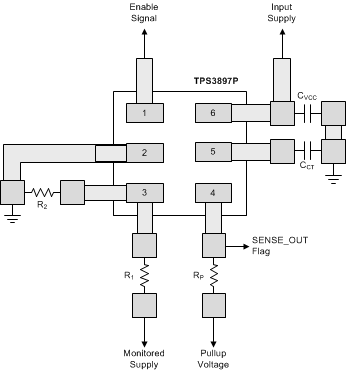
TPS389 pcb_layout_dry_bvs172.gifFigure 31. TPS3897P Layout Example (DRY Package)