ZHCSG28B March   2017  – February 2018 TPS3890-Q1

PRODUCTION DATA.  

  1. 特性
  2. 应用
  3. 说明
    1.     Device Images
      1.      典型应用电路
      2.      VITN 精度与温度间的关系
  4. 修订历史记录
  5. Device Comparison Table
  6. Pin Configuration and Functions
    1.     Pin Functions
  7. Specifications
    1. 7.1 Absolute Maximum Ratings
    2. 7.2 ESD Ratings
    3. 7.3 Recommended Operating Conditions
    4. 7.4 Thermal Information
    5. 7.5 Electrical Characteristics
    6. 7.6 Timing Requirements
    7. 7.7 Typical Characteristics
  8. Detailed Description
    1. 8.1 Overview
    2. 8.2 Functional Block Diagram
    3. 8.3 Feature Description
      1. 8.3.1 User-Configurable RESET Delay Time
      2. 8.3.2 Manual Reset (MR) Input
      3. 8.3.3 RESET Output
      4. 8.3.4 SENSE Input
        1. 8.3.4.1 Immunity to SENSE Pin Voltage Transients
    4. 8.4 Device Functional Modes
      1. 8.4.1 Normal Operation (VDD > VDD(min))
      2. 8.4.2 Above Power-On-Reset But Less Than VDD(min) (VPOR < VDD < VDD(min))
      3. 8.4.3 Below Power-On-Reset (VDD < VPOR)
  9. Application and Implementation
    1. 9.1 Application Information
    2. 9.2 Typical Application
      1. 9.2.1 Design Requirements
      2. 9.2.2 Detailed Design Procedure
      3. 9.2.3 Application Curve
  10. 10Power Supply Recommendations
  11. 11Layout
    1. 11.1 Layout Guidelines
    2. 11.2 Layout Example
  12. 12器件和文档支持
    1. 12.1 器件支持
      1. 12.1.1 器件命名规则
    2. 12.2 文档支持
      1. 12.2.1 相关文档
    3. 12.3 接收文档更新通知
    4. 12.4 社区资源
    5. 12.5 商标
    6. 12.6 静电放电警告
    7. 12.7 Glossary
  13. 13机械、封装和可订购信息

封装选项

机械数据 (封装 | 引脚)
散热焊盘机械数据 (封装 | 引脚)
订购信息

Typical Characteristics

over the operating junction temperature range of –40°C to +125°C, 1.5 V ≤ VDD ≤ 5.5 V, and MR = VDD (unless otherwise noted)
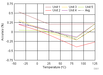
TPS3890-Q1 D001-SLVSD65-01_Vit-.gif
Figure 2. VITN Accuracy vs Temperature
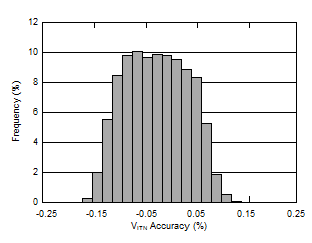
TPS3890-Q1 D019_SLVSD65_Vitp_Histogrom.gif
Tested at VDD = 1.5 V and VDD = 5.5 V, total tests = 136,348
Figure 4. VITN Accuracy Histogram
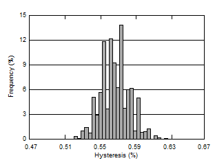
TPS3890-Q1 D021_SLVSD65_Hyst_Histogrom.gif
Tested at VDD = 1.5 V and VDD = 5.5 V, total tests = 136,348
Figure 6. Hysteresis Histogram
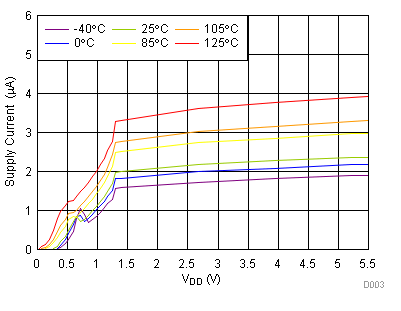
TPS3890-Q1 D003-SLVSD65-01_Iq_MR_6p5V.gif
MR = VDD
Figure 8. Supply Current vs Power-Supply Voltage
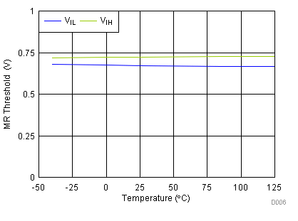
TPS3890-Q1 D006-SLVSD65-03_MR_Thresh_VCC_1p5V.gif
VDD = 1.5 V
Figure 10. MR Threshold vs Temperature
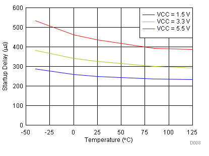
TPS3890-Q1 D008-SLVSD65-01_Startup_Delay.gif
Figure 12. Startup Delay vs Temperature
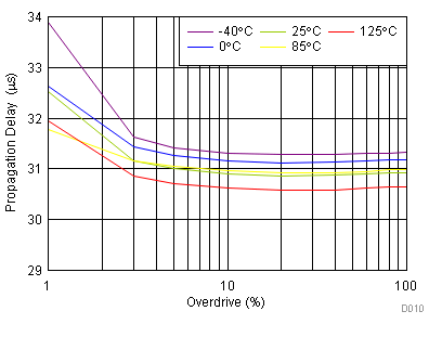
TPS3890-Q1 D010-SLVSD65-01_Prop_Delay_LH_1p5V.gif
VDD = 1.5 V
Figure 14. Propagation Delay (tPD(r)) vs Overdrive
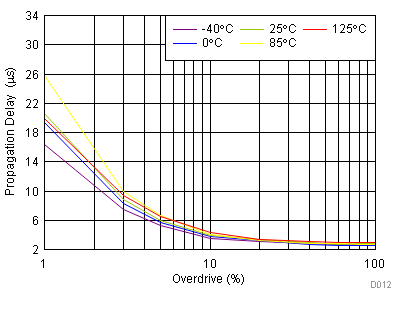
TPS3890-Q1 D012-SLVSD65-01_Prop_Delay_HL_1p5V.gif
VDD = 1.5 V
Figure 16. Propagation Delay (tPD(f)) vs Overdrive
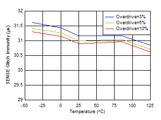
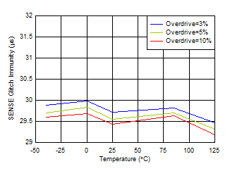
TPS3890-Q1 D014-SLVSD65-01_Glitch_Rejection_1p5V.gif
VDD = 1.5 V
Figure 18. Low-to-High Glitch Immunity vs Temperature
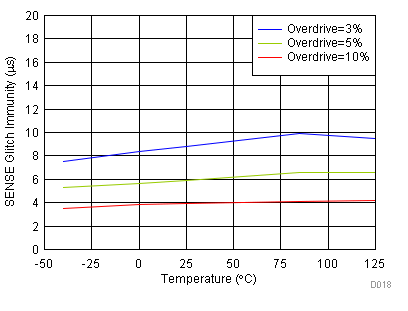
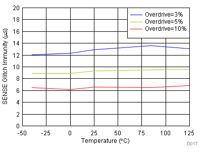
TPS3890-Q1 D018-SLVSD65-04.gif
VDD = 1.5 V
Figure 20. High-to-Low Glitch Immunity vs Temperature
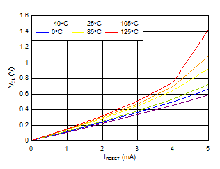
TPS3890-Q1 D016-SLVSD65-01_Vol_1p5.gif
VDD = 1.5 V
Figure 22. Low-Level Output Voltage vs RESET Current
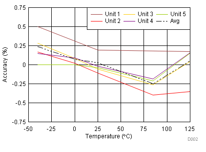
TPS3890-Q1 D002-SLVSD65-01_Vit_plus.gif
Figure 3. VITP Accuracy vs Temperature
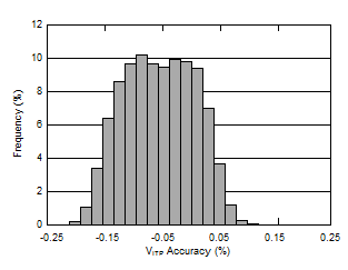
TPS3890-Q1 D020_SLVSD65_Vitn_Histogrom.gif
Tested at VDD = 1.5 V and VDD = 5.5 V, total tests = 136,348
Figure 5. VITP Accuracy Histogram
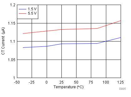
TPS3890-Q1 D005-SLVSD65-01_CT_Current.gif
Figure 7. CT Current vs Temperature
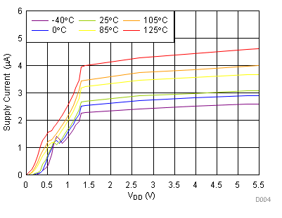
TPS3890-Q1 D004-SLVSD65-02_Iq_MR_0V.gif
MR = 0 V
Figure 9. Supply Current vs Power-Supply Voltage
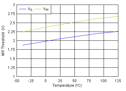
TPS3890-Q1 D007-SLVSD65-01_MR_Thresh_VCC_6p5V.gif
VDD = 5.5 V
Figure 11. MR Threshold vs Temperature
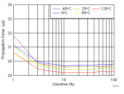
TPS3890-Q1 D009-SLVSD65-02_Prop_Delay_LH_6p5V.gif
VDD = 5.5 V
Figure 13. Propagation Delay (tPD(r)) vs Overdrive
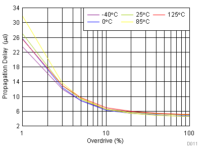
TPS3890-Q1 D011-SLVSD65-02_Prop_Delay_HL_6p5V.gif
VDD = 5.5 V
Figure 15. Propagation Delay (tPD(f)) vs Overdrive
TPS3890-Q1 D013-SLVSD65-01_Glitch_Rejection_6p5V.gif
VDD = 5.5 V
Figure 17. Low-to-High Glitch Immunity vs Temperature
TPS3890-Q1 D017-SLVSD65-01.gif
VDD = 5.5 V
Figure 19. High-to-Low Glitch Immunity vs Temperature
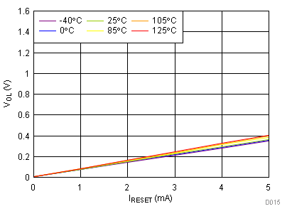
TPS3890-Q1 D015-SLVSD65-02_Vol_5p5.gif
VDD = 5.5 V
Figure 21. Low-Level Output Voltage vs RESET Current